DESCRIPTION
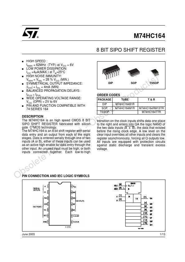
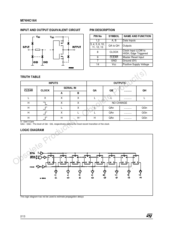
s Data is entered serially through one of two c inputs (A or B), either of these inputs can be used u as an active high enable for data entry through the d other input. An unused input must be high, or both ro inputs connected together. A low level on the clear input overrides all other inputs and clears the register asynchronously, forcing all Q outputs low. All inputs are equipped with protection circuits against static discharge and transient excess voltage. Obsolete P PIN CONNECTION AND IEC LOGIC SYMBOLS June 2003 1/13 M74HC164 INPUT AND OUTPUT EQUIVALENT CIRCUIT PIN DESCRIPTION
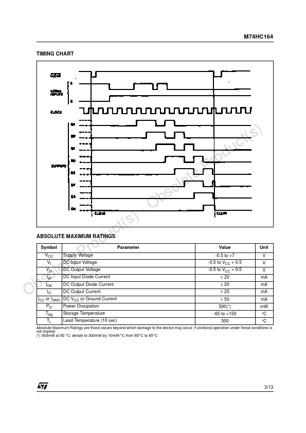
PIN No 1,2 3, 4, 5, 6, 10, 11, 12, 13 8 9 7 14 SYMBOL A, B QA to QH CLOCK CLEAR GND Vcc NAME AND FUNCTION Data Inputs Outputs Clock Input (LOW to HIGH, Edge Triggered Master Reset Input Ground (0V) Positive Supply Voltage t(s) TRUTH TABLE c INPUTS OUTPUTS rodu CLEAR CLOCK SERIAL IN A B QA QB ........... P L X X X L L ........... lete H X X NO CHANGE o H L X L QAn ........... bs H X L L QAn ........... STMicroelectronics