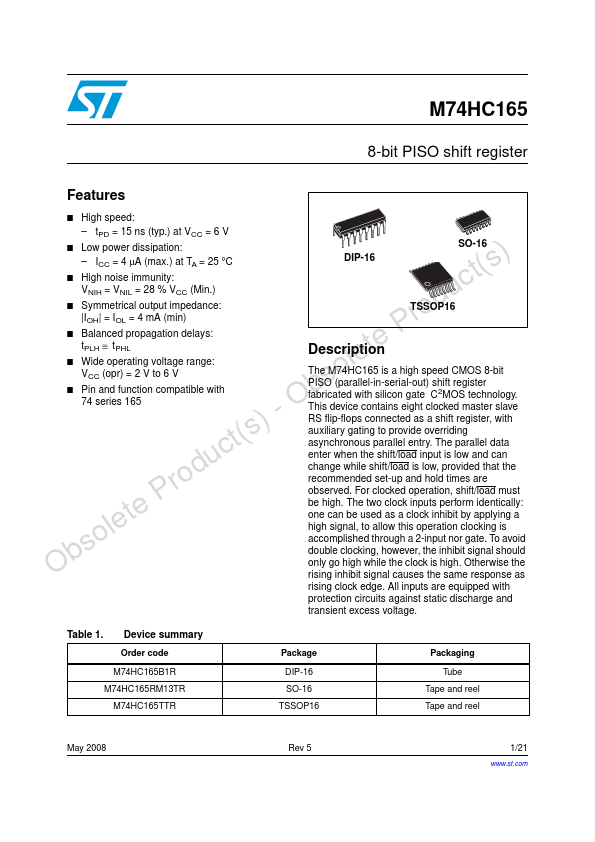
DESCRIPTION
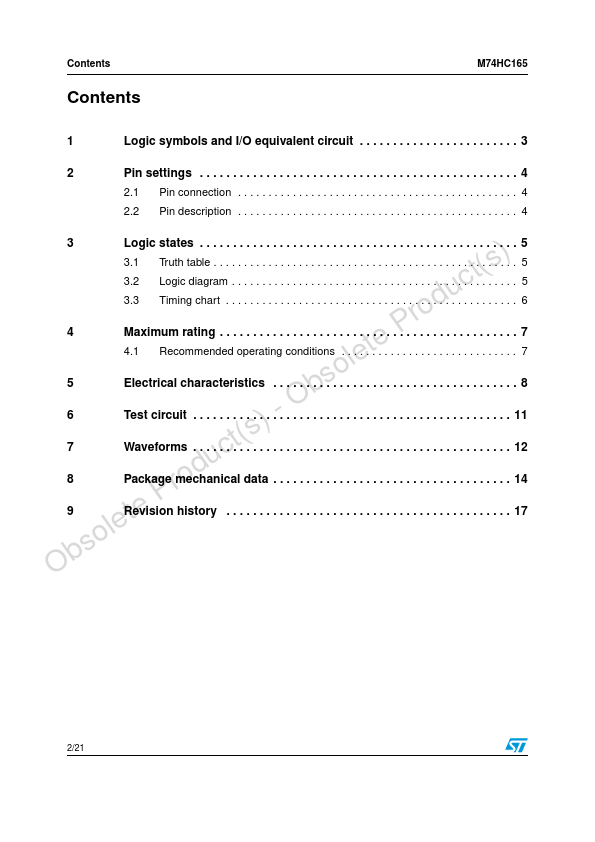
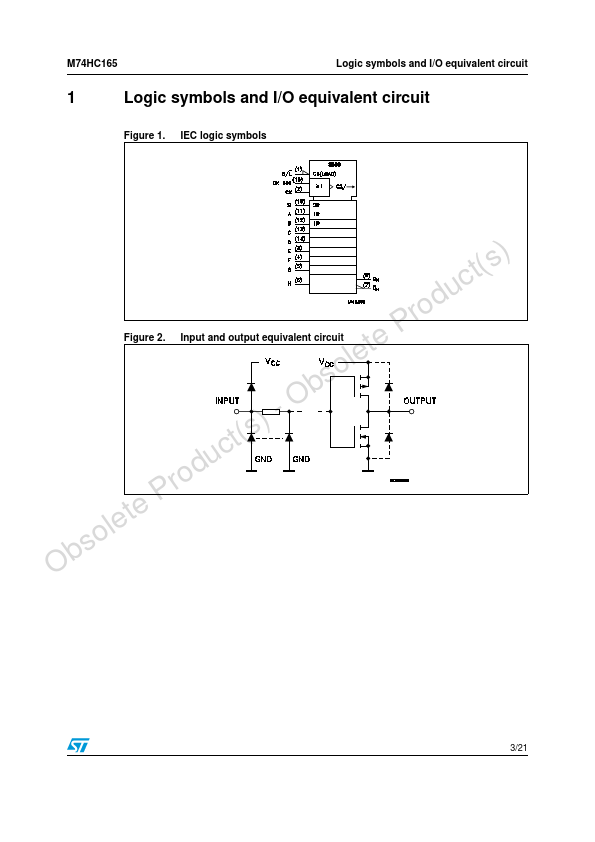
Parallel data enters when the shift/load input is low. For clocked operation, shift/load must be high. The two clock input perform identically; one can be used as a clock inhibit by applying a high signal; to permit this operation clocking is accomplished through a 2 input nor gate. To avoid double clocking, however, the inhibit signal should only go high while the clock is high. Otherwise the rising inhibit signal will cause the same response as rising clock edge. All inputs are equipped with protection circuits against static discharge and transient excess voltage. PIN CONNECTION AND IEC LOGIC SYMBOLS July 2001 1/12 M74HC165 INPUT AND OUTPUT EQUIVALENT CIRCUIT PIN DESCRIPTION
PIN No 1 2 7 9 SYMBOL NAME AND FUNCTION 10 11, 12, 13, A to H 14, 3, 4, 5, 6 15 CLOCK INH 8 GND 16 Vcc SHIFT/LOAD Data Inputs Complementary Output QH QH Serial Output Clock Input (LOW to CLOCK HIGH, Edge Triggered SI Serial Data Inputs Parallel Data Inputs Clock Inhibit Ground (0V) Positive Supply Vo... STMicroelectronics