DESCRIPTION
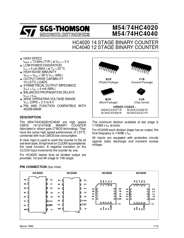
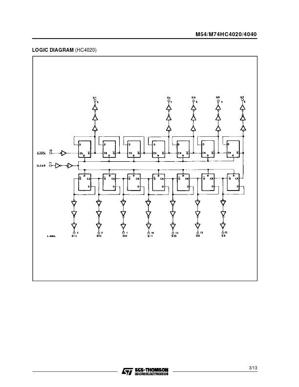
A clear input is used to reset the counter to the all low level state. A high level on CLEAR accomplishes the reset function. A negative transition on the CLOCK input increments the counter by one. For HC4020 twelve kind od divided output are provided; 1st and 4th stage to 14th stage. PIN CONNECTION (top view) HC4020 HC4040 HC4020 HC4040 The maximum division available at last stage is 1/16384 x fIN at clock. For HC4040 each division stage has an output; the final frequency is 1/4096 x fIN. All inputs are equipped with protection circuits against static discharge and transient excess voltage. March 1993 1/13 M54/M74HC4020/4040 INPUT AND OUTPUT EQUIVALENT CIRCUIT PIN DESCRIPTION
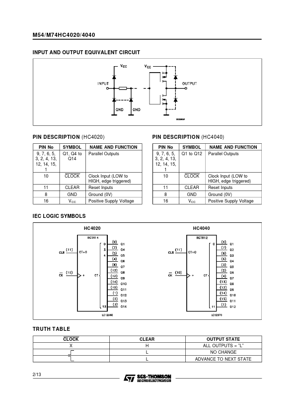
(HC4020) PIN No 9, 7, 6, 5, 3, 2, 4, 13, 12, 14, 15, 1 10 11 8 16 SYMBOL Q1, Q4 to Q14 NAME AND FUNCTION Parallel Outputs PIN DESCRIPTION
(HC4040) PIN No 9, 7, 6, 5, 3, 2, 4, 13, 12, 14, 15, 1 10 11 8 16 SYMBOL Q1 to Q12 NAME AND FUNCTION Parallel Outputs CLOCK CLEAR GND V CC Clock Input (LOW to HIGH,... STMicroelectronics