STB21NM60N-1 Overview
Key Specifications
Package: TO-262-3
Mount Type: Through Hole
Pins: 3
Max Operating Temp: 150 °C
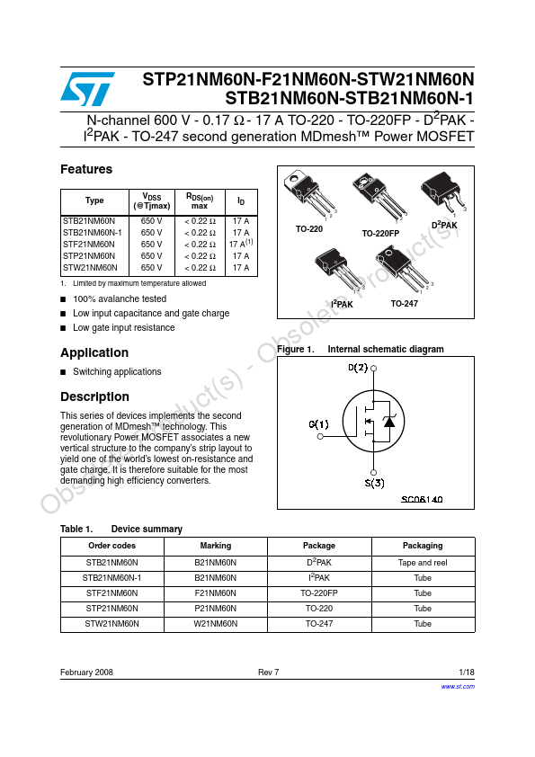
Key Features
- 100% avalanche tested te
- Low input capacitance and gate charge le
- Low gate input resistance bsoApplication
- Internal Table
- STB21NM60N-1 - STW21NM60N 1 Electrical ratings . . . . . . . . . . . . . . . . . . . . . . . . . . . . . . . . . . . . . . . . . . . . 3