STB33N60M2
Key Features
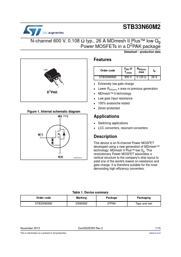
- 2 PAK 3 Figure
- Internal schematic diagram , TAB AM15572v1 Order code STB33N60M2 VDS @ TJmax 650 V RDS(on) max
- 125 Ω ID 26 A
- Extremely low gate charge
- Lower RDS(on) x area vs previous generation
- MDmesh™ II technology
- Low gate input resistance
- 100% avalanche tested
- Zener-protected