STB8NC70Z-1
STB8NC70Z-1 is N-CHANNEL MOSFET manufactured by STMicroelectronics.
- Part of the STB8NC70Z comparator family.
- Part of the STB8NC70Z comparator family.
N The third generation of MESH OVERLAY™ Power MOSFETs for very high voltage exhibits unsurpassed on-resistance per unit area while integrating back-toback Zener diodes between gate and source. Such arrangement gives extra ESD capability with higher ruggedness performance as requested by a large variety of single-switch applications. APPLICATIONS SINGLE-ENDED SMPS IN MONITORS, PUTER AND INDUSTRIAL APPLICATION s WELDING EQUIPMENT s
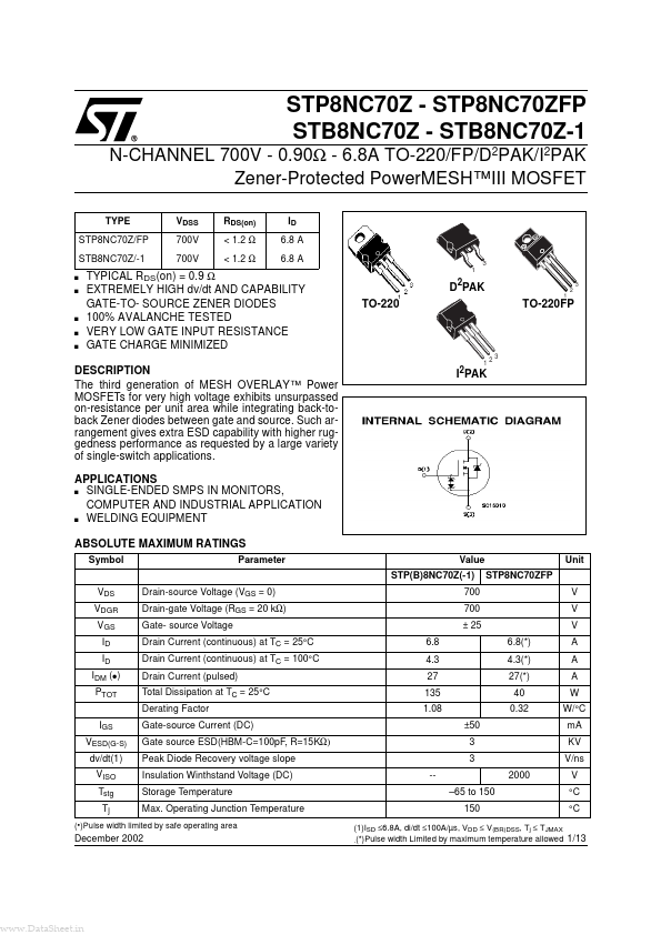
I2PAK
ABSOLUTE MAXIMUM RATINGS
Symbol VDS VDGR VGS ID ID IDM (q ) PTOT IGS VESD(G-S) dv/dt(1) VISO Tstg Tj Parameter Drain-source Voltage (VGS = 0) Drain-gate Voltage (RGS = 20 kΩ) Gate- source Voltage Drain Current (continuous) at TC = 25°C Drain Current (continuous) at TC = 100°C Drain Current (pulsed) Total Dissipation at TC = 25°C Derating Factor Gate-source Current (DC) Gate source ESD(HBM-C=100p F, R=15KΩ) Peak Diode Recovery voltage slope Insulation Winthstand Voltage (DC) Storage Temperature Max. Operating Junction Temperature
.(- )Pulse
Value STP(B)8NC70Z(-1) 700 700 ± 25 6.8 4.3 27 135 1.08 ±50 3 3 -- 65 to 150 150 2000 6.8(- ) 4.3(- ) 27(- ) 40 0.32 STP8NC70ZFP
Unit V V V A A A W W/°C m A KV V/ns V °C °C
(- )Pulse width limited by safe operating area
December 2002
(1)ISD ≤6.8A, di/dt ≤100A/µs, VDD ≤ V(BR)DSS, Tj ≤ TJMAX width Limited by maximum temperature allowed 1/13
.Data Sheet.in
STP8NC70Z
- STP8NC70ZFP
- STB8NC70Z
- STB8NC70Z-1
THERMAL DATA
TO-220 / D2PAK I2PAK Rthj-case Rthj-amb Tl Thermal Resistance Junction-case Max Thermal Resistance Junction-ambient Max Maximum Lead Temperature For Soldering Purpose 0.93 62.5 300 TO-220FP 3.13 °C/W °C/W °C
AVALANCHE CHARACTERISTICS
Symbol IAR EAS Parameter Avalanche Current, Repetitive or Not-Repetitive (pulse width limited by Tj max) Single Pulse Avalanche Energy (starting Tj = 25 °C, ID = IAR, VDD = 50 V) Max Value 6.8 354 Unit A m J
ELECTRICAL CHARACTERISTICS (TCASE = 25 °C UNLESS OTHERWISE SPECIFIED) OFF
Symbol V(BR)DSS Parameter Drain-source Breakdown Voltage Test...