VN31SP
VN31SP is HIGH SIDE SMART POWER SOLID STATE RELAY manufactured by STMicroelectronics.
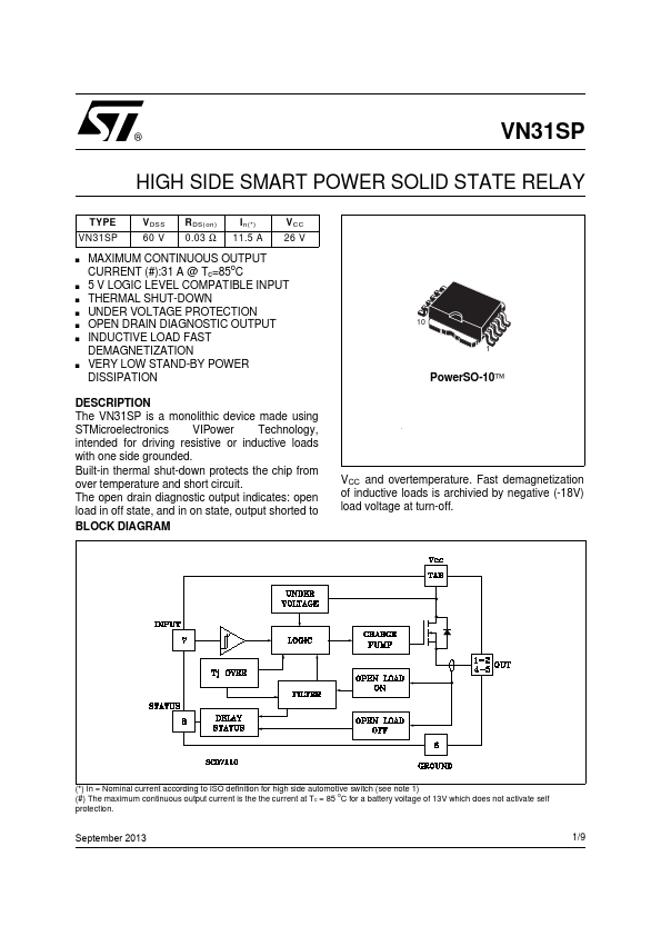
DESCRIPTION
The VN31SP is a monolithic device made using STMicroelectronics VIPower Technology, intended for driving resistive or inductive loads with one side grounded.
Built-in thermal shut-down protects the chip from over temperature and short circuit. The open drain diagnostic output indicates: open load in off state, and in on state, output shorted to
BLOCK DIAGRAM
10 1
Power SO-10™
VCC and overtemperature. Fast demagnetization of inductive loads is archivied by negative (-18V) load voltage at turn-off.
(- ) In = Nominal current according to ISO definition for high side automotive switch (see note 1) (#) The maximum continuous output current is the the current at Tc = 85 o C for a battery voltage of 13V which does not activate self protection.
September 2013
1/9
ABSOLUTE MAXIMUM RATING
Symbol V(BR)DSS
IOUT IR IIN
-VCC ISTAT VESD Ptot
Tj Tstg
Parameter Drain-Source Breakdown Voltage Output Current (cont.) at Tc = 85 o C Reverse Output Current at Tc = 85 o C Input Current Reverse Supply Voltage Status Current Electrostatic Discharge (1.5 kΩ, 100 p F) Power Dissipation at Tc = 85 o C Junction Operating Temperature Storage Temperature
CONNECTION DIAGRAMS
Value 60 31 -31 ±10 -4 ±10
2000 54
-40 to 150 -55 to 150
Unit V A A m A V m A V W o C o C
CURRENT AND VOLTAGE CONVENTIONS
2/9
THERMAL DATA
Rthj-case Thermal Resistance Junction-case Rthj-amb Thermal Resistance Junction-ambient ($)
Max
1.2 o C/W
Max
50 o C/W
($) When mounted using minimum remended pad size on FR-4 board
ELECTRICAL CHARACTERISTICS (VCC = 13 V; -40 ≤ Tj ≤ 125 o C unless otherwise specified) POWER
Symbol VCC In(- ) Ron
VDS(MAX)
Parameter
Test Conditions
Supply Voltage Nominal Current
Tc = 85 o C VDS(on) ≤ 0.5 (note 1)
On State Resistance
IOUT = 11.5 A IOUT = 11.5...