VN330SP
VN330SP is QUAD HIGH SIDE SMART POWER SOLID STATE RELAY manufactured by STMicroelectronics.
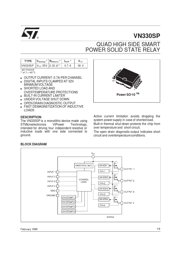
DESCRIPTION
The VN330SP is a monolithic device made using STMicroelectronics VIPower Technology, intended for driving four indipendent resistive or inductive loads with one side connected to ground. BLOCK DIAGRAM
Active current limitation avoids dropping the system power supply in case of shorted load. Built-in thermal shut-down protects the chip from over temperature and short circuit. The open drain diagnostic output indicates short circuit and overtemperature conditions.
February 1999
1/9
ABSOLUTE MAXIMUM RATING
Symb ol VCC -V CC I OUT IR I IN I DIAG V ESD E AS P tot Tj T s tg Power Supply Voltage Reverse Supply Voltage Output Current (cont.) Reverse Output Current (per channel) Input Current (per channel) DIAG Pin Current Electrostatic Discharge (1.5 k Ω, 100 p F) Single Pulse Avalanche Energy per Channel Not Symultaneously (see figure 1) Power Dissipation at T c ≤ 25 C Junction Operating Temperature Storage Temperature o
Parameter
Value 45 -0.3 Internally Limited -6 ± 10 ± 10 2000 400 Internally Limited Internally Limited -55 to 150
Unit V V A A m A m A V m J W o o
CONNECTION DIAGRAM
CURRENT AND VOLTAGE CONVENTIONS
2/9
THERMAL DATA
R t hj-ca se R t hj- amb Thermal Resistance Junction-case (1) Thermal Resistance Junction-ambient ($) Max Max 2 50 o o
C/W C/W
(1) All channels ON ($) When mounted using minimum remended pad size on FR-4 board
ELECTRICAL CHARACTERISTICS (10 V < VCC < 36 V; -25 o C < TJ < 125 o C unless otherwise specified) POWER
Symb ol VCC R on IS V demag Parameter Supply Voltage On State Resistance Supply Current Output Voltage at Turn-Off I OUT = 0.5 A I OUT = 0.5 A T J = 125 C T J = 85 o C o
Test Cond ition s
Min. 10
Typ .
Max. 36 0.4 0.32 1 10
Un it V Ω Ω m A m A V
All Channels O ff o On State (Tj =125 C) I out1 .. Io ut4 =0 I out = 0.5A LLOAD = 1 m H
V CC -65 VCC -55 V CC -45
SWITCHING (VCC = 24 V)
Symb ol t d(on) Parameter Turn-on Delay Time Of Output Current Test Cond ition s I OUT = 0.5 A Resistive Load...