STMicroelectronics XSD56120
The SD56120 is a common source N-Channel enhancement-mode lateral Field-Effect RF power transistor designed for broadband commercial and industrial applications at frequencies up to 1.0 GHz. The SD56120 is designed for high gain and broadband performance operating in common source mode at 28V.| Part No. | XSD56120 |
|---|---|
| Datasheet | XSD56120 Download |
| Manufacturer |  STMicroelectronics |
| Description | RF POWER TRANSISTORS RF POWER TRANSISTORS |
| Buy | Stock & Price |
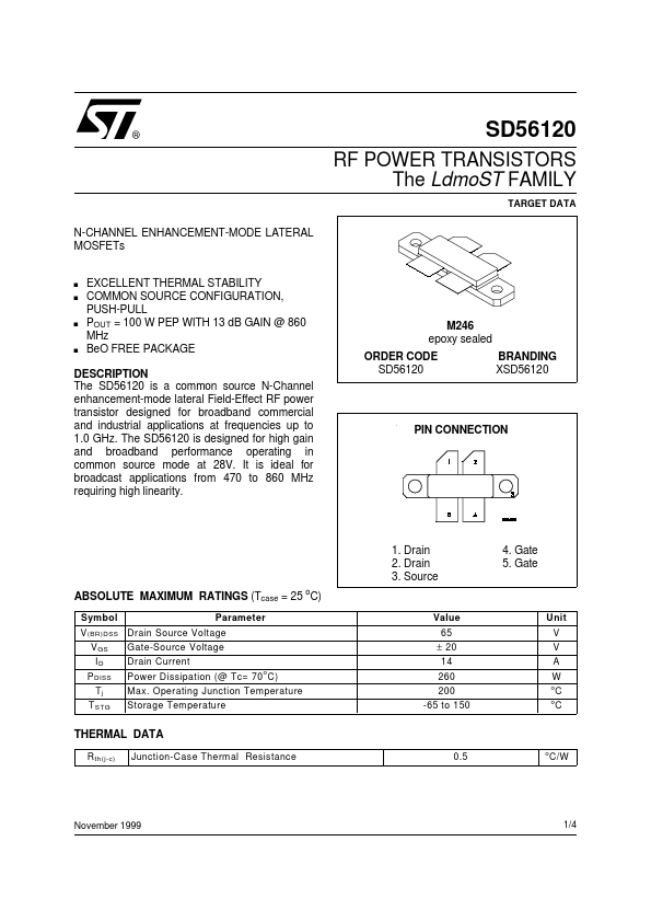
DESCRIPTION
It is ideal for broadcast applications from 470 to 860 MHz requiring high linearity. PIN CONNECTION 1. Drain 2. Drain 3. SourceABSOLUTE MAXIMUM RATINGS
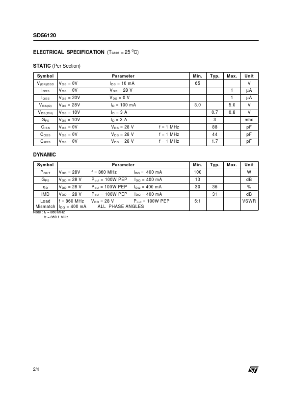
(Tcase = 25 oC) Symbol V GS ID P DISS Tj T STG Parameter Gate-Source Voltage Drain Current Power Dissipation (@ Tc= 70 o C) Max. Operating Junction Temperature Storage Temperature Value 65 ± 20 14 260 200 -65 to 150 4. Gate 5. Gate Unit V V A W o o V (BR)DSS Drain Source Voltage C C THERMAL DATA R th(j-c) Junction-Case Thermal Resistance 0.5 o C/W November 1999 1/4 SD56120 ELECTRICAL SPECIFICATION (Tcase = 25 oC) STATIC (Per Section) Symbol V (BR)DSS I DSS I GSS V GS(Q) V DS(ON) G FS C ISS C OSS C RSS V GS = 0V V GS = 0V V GS = 20V V DS = 28V V GS = 10V V DS = 10V V GS = 0V V GS = 0V V GS = 0V Parameter I DS = 10 mA V DS = 28 V V DS = 0 V I D = 100 mA ID = 3 A ID = 3 A V DS = 28 V V DS = 28 V V DS = 28 V f = 1 MHz f = 1 MHz f = 1 MHz 3.0 0.7 3 88 44 1.7 Min. 65 1 1 5.0 0.8 Typ. Max. Unit V µA µA V V mho pF pF pF DYNAMIC Sym...