STM4470
STM4470 is N-Channel MOSFET manufactured by SamHop Microelectronics.
Green Product
Oct. 16. 2006 Ver1.1
SamHop Microelectronics Corp.
N-Channel Enhancement Mode Field Effect Transistor
PRODUCT SUMMARY
VDSS
40V d
Features
( m Ω ) Max
10A
RDS(ON)
Super high dense cell design for low RDS(ON).
10 @ VGS = 10V 13 @ VGS = 4.5V
Rugged and reliable. Surface Mount Package.
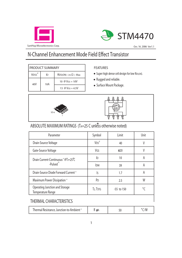
SO-8...