STM4470E
STM4470E is N-channel Enhancement Mode Field Effect Transistor manufactured by SamHop Microelectronics.
SamHop Microelectronics Corp.
May. 15 2007 ver1.0
N-Channel Enhancement Mode Field Effect Transistor
PRODUCT SUMMARY
VDSS
40V
F E AT UR E S S uper high dense cell design for low R DS (ON ).
9.5A
RDS(ON) ( m ı Ω ) Max
12 @ VGS = 10V 15 @ VGS = 4.5V
R ugged and reliable. S urface Mount P ackage. E S D P rotected.
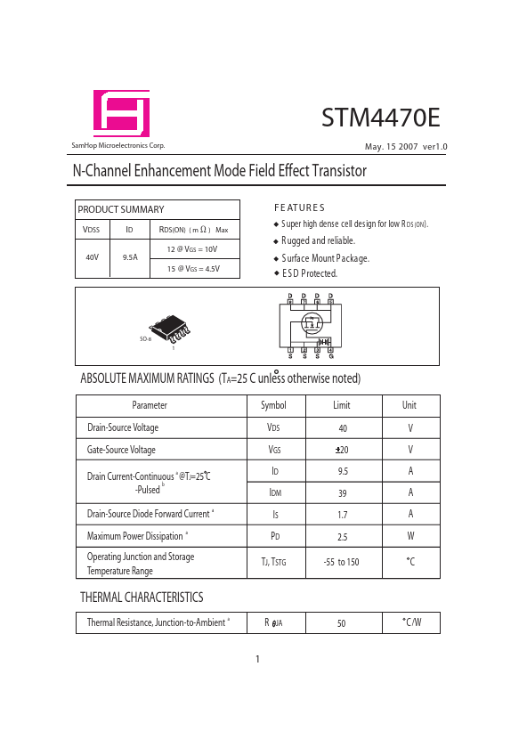
SO-8...