STS3411A
STS3411A is P-Channel Enhancement Mode Field Effect Transistor manufactured by SamHop Microelectronics.
STS3411AGreen
Product
Sa mHop Microelectronics C orp.
P-Channel Enhancement Mode Field Effect Transistor
Ver 1.0
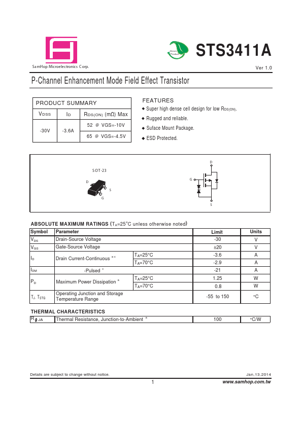
PRODUCT SUMMARY
VDSS
ID RDS(ON) (mΩ) Max
-30V
-3.6A
52 @ VGS=-10V 65 @ VGS=-4.5V
Features
Super high dense cell design for low RDS(ON). Rugged and reliable. Suface Mount Package. ESD Protected.
S...