STS3415
STS3415 is P-Channel Enhancement Mode Field Effect Transistor manufactured by SamHop Microelectronics.
Gr Pr
Ver 2.0
S a mHop Microelectronics C orp.
P-Channel Enhancement Mode Field Effect Transistor
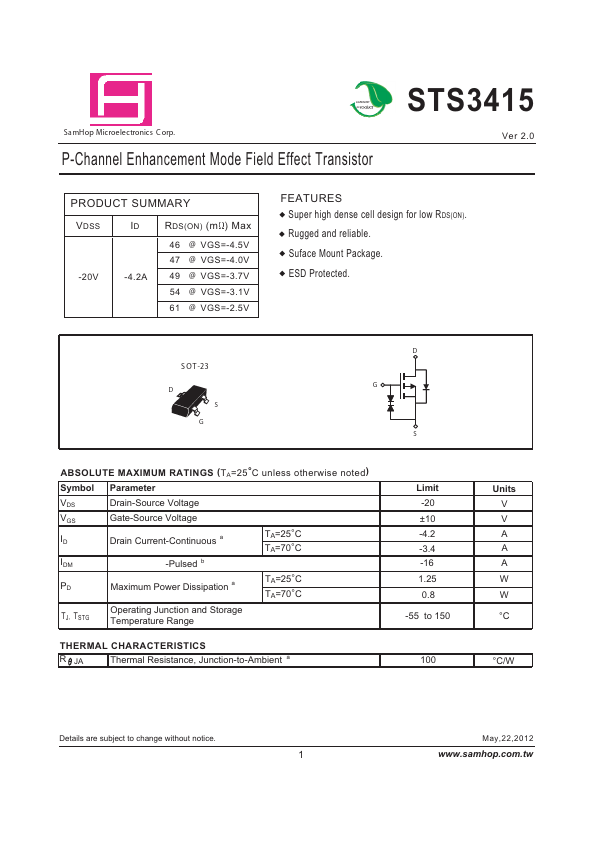
PRODUCT SUMMARY
V DSS ID R DS(ON) (m Ω) Max
46 @ VGS=-4.5V 47 @ VGS=-4.0V -20V -4.2A 49 @ VGS=-3.7V 54 @ VGS=-3.1V 61 @ VGS=-2.5V
Features
Super high dense cell design for low R DS(ON). Rugged and reliable. Suface Mount Package. ESD Protected.
S OT -23
D S G S...