Datasheet4U Logo Datasheet4U.com

K7P323688M - 1Mx36 & 2Mx18 SRAM

Datasheet Summary

Description

Pin Name K, K SAn DQn SS SW SWa SWb SWc SWd M 1 , M2 G Pin Description Differential Clocks Synchronous Address Input Bi-directional Data Bus Synchronous Select Synchronous Global Write Enable Synchronous Byte a Write Enable Synchronous Byte b Write Enable Synchronous Byte c Write Enable Synchronous

Features

  • 1Mx36 or 2Mx18 Organizations.
  • 1.8V VDD/1.5V or 1.8V VDDQ.
  • HSTL Input and Output Levels.
  • Differential, HSTL Clock Inputs K, K.
  • Synchronous Read and Write Operation.
  • Registered Input and Registered Output.
  • Internal Pipeline Latches to Support Late Write.
  • Byte Write Capability(four byte write selects, one for each 9bits).
  • Synchronous or Asynchronous Output Enable.
  • Power Down Mode via ZZ Signal.

📥 Download Datasheet

Datasheet preview – K7P323688M

Datasheet Details

Part number K7P323688M
Manufacturer Samsung Electronics
File Size 419.16 KB
Description 1Mx36 & 2Mx18 SRAM
Datasheet download datasheet K7P323688M Datasheet
Additional preview pages of the K7P323688M datasheet.
Other Datasheets by Samsung Electronics

Full PDF Text Transcription

Click to expand full text
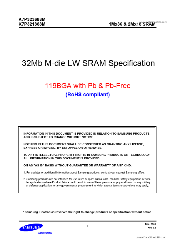
K7P323688M K7P321888M 1Mx36 & 2Mx18 SRAM www.DataSheet4U.com 32Mb M-die LW SRAM Specification 119BGA with Pb & Pb-Free (RoHS compliant) INFORMATION IN THIS DOCUMENT IS PROVIDED IN RELATION TO SAMSUNG PRODUCTS, AND IS SUBJECT TO CHANGE WITHOUT NOTICE. NOTHING IN THIS DOCUMENT SHALL BE CONSTRUED AS GRANTING ANY LICENSE, EXPRESS OR IMPLIED, BY ESTOPPEL OR OTHERWISE, TO ANY INTELLECTUAL PROPERTY RIGHTS IN SAMSUNG PRODUCTS OR TECHNOLOGY. ALL INFORMATION IN THIS DOCUMENT IS PROVIDED ON AS "AS IS" BASIS WITHOUT GUARANTEE OR WARRANTY OF ANY KIND. 1. For updates or additional information about Samsung products, contact your nearest Samsung office. 2.
Published: |