K3N5VU1000F-DC
K3N5VU1000F-DC is 16M-Bit (2Mx8 / 1Mx16) CMOS Mask ROM manufactured by Samsung Semiconductor.
- Part of the K3N5V1000F-DC comparator family.
FEATURES
- Switchable organization 2,097,152 x 8(byte mode) 1,048,576 x 16(word mode)
- Fast access time 3.3V Operation : 100ns(Max.)@CL=50p F, 120ns(Max.)@CL=100p F 3.0V Operation : 120ns(Max.)@CL=100p F
- Supply voltage : single +3.0V/single +3.3V ..
- Current consumption Operating : 40m A(Max.) Standby : 30µA(Max.)
- Fully static operation
- All inputs and outputs TTL patible
- Three state outputs
- Package -. K3N5V(U)1000F-DC : 42-DIP-600 -. K3N5V(U)1000F-GC : 44-SOP-600
CMOS MASK ROM
GENERAL DESCRIPTION
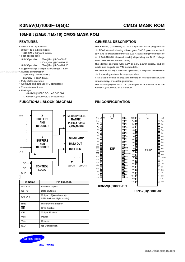
The K3N5V(U)1000F-D(G)C is a fully static mask programmable ROM fabricated using silicon gate CMOS process technology, and is organized either as 2,097,152 x 8 bit(byte mode) or as 1,048,576x16 bit(word mode) depending on BHE voltage level.(See mode selection table) This device operates with 3.0V or 3.3V power supply, and all inputs and outputs are TTL patible. Because of its asynchronous operation, it requires no external clock assuring extremely easy operation. It is suitable for use in program memory of microprocessor, and data memory, character generator. The K3N5V(U)1000F-DC is packaged in a 42-DIP and the K3N5V(U)1000F-GC in a 44-SOP.
FUNCTIONAL BLOCK DIAGRAM
PIN CONFIGURATION
A19
- . . . A0 A-1
X BUFFERS AND DECODER
MEMORY CELL MATRIX (1,048,576x16/ 2,097,152x8)
A18 A17 A7 A6 A5 A4 A3
1 2 3 4 5 6 7 8 9
42 A19 41 A8 40 A9 39 A10 38 A11 37 A12 36 A13 35 A14 34 A15 33 A16 32 BHE
N.C 1 A18 A17 A7 2 3 4
44 N.C 43 A19 42 A8 41 A9 40 A10 39 A11 38 A12 37 A13 36 A14 35 A15 34 A16 33 BHE 32 VSS 31 Q15 /A-1 30 Q7 29 Q14 28 Q6 27 Q13 26 Q5 25 Q12 24 Q4 23 VCC
A6 5 A5 6 A4 A3 A2 7 8 9
Y BUFFERS AND DECODER
SENSE AMP. DATA OUT BUFFERS . . .
A2 A1
A0 10 CE 11 VSS 12 OE 13 Q0 14 Q8 15 Q1 16
A1 10 A0 11
CE OE BHE CONTROL LOGIC Q0/Q8 Q7/Q15
Q9 17 Q2 18 Q10 19 Q3 20 Q11 21
]
Pin Name A0
- A19 Q0
- Q14 Q15 /A-1 BHE CE OE VCC VSS N.C Pin Function Address Inputs Data Outputs Output 15(Word mode)/ LSB Address(Byte mode) Word/Byte selection Chip...