Datasheet4U Logo Datasheet4U.com
Samsung Semiconductor logo

K4X56163PE Datasheet

Manufacturer: Samsung Semiconductor
K4X56163PE datasheet preview

Datasheet Details

Part number K4X56163PE
Datasheet K4X56163PE_Samsungsemiconductor.pdf
File Size 698.98 KB
Manufacturer Samsung Semiconductor
Description 16M x16 Mobile DDR SDRAM
K4X56163PE page 2 K4X56163PE page 3

K4X56163PE Overview

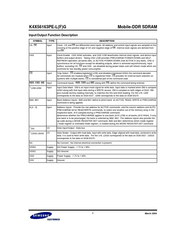
SYMBOL CK, CK TYPE Input DESCRIPTION Mobile-DDR SDRAM Clock : CK and CK are differential clock inputs. All address and control input signals are sampled on the crossing of the positive edge of CK and negative edge of CK.

K4X56163PE Key Features

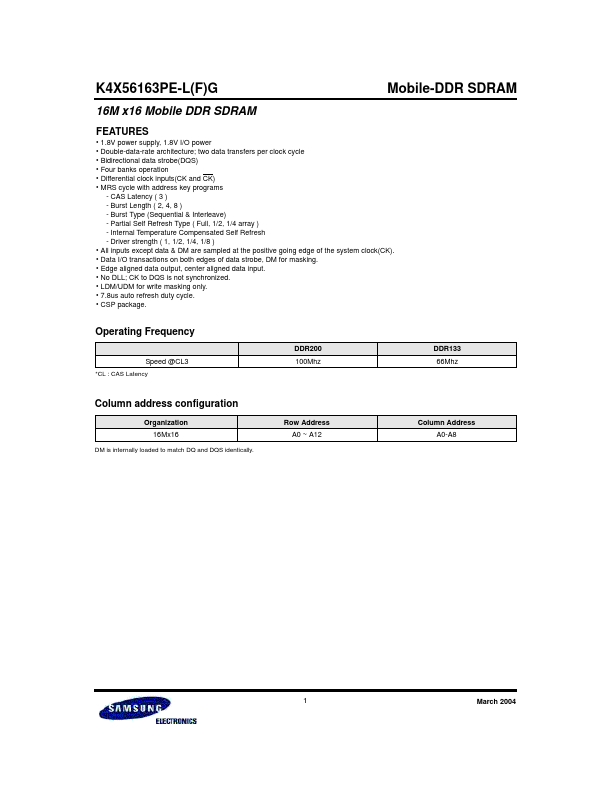
  • 1.8V power supply, 1.8V I/O power
  • Double-data-rate architecture; two data transfers per clock cycle
  • Bidirectional data strobe(DQS)
  • Four banks operation
  • Differential clock inputs(CK and CK)
  • MRS cycle with address key programs
  • CAS Latency ( 3 )
  • Burst Length ( 2, 4, 8 )
  • Burst Type (Sequential & Interleave)
  • Partial Self Refresh Type ( Full, 1/2, 1/4 array )
Samsung Semiconductor logo - Manufacturer

More Datasheets from Samsung Semiconductor

See all Samsung Semiconductor datasheets

Part Number Description
K4X56163PE-LFG 16M x16 Mobile DDR SDRAM
K4X56163PE-LG 16M x16 Mobile DDR SDRAM
K4X56163PG-FE 16M x16 Mobile-DDR SDRAM
K4X56163PG-FG 16M x16 Mobile-DDR SDRAM
K4X56163PG-LE 16M x16 Mobile-DDR SDRAM
K4X56163PG-LG 16M x16 Mobile-DDR SDRAM
K4X56163PI-FE 16Mx16 Mobile DDR SDRAM
K4X56163PI-FG 16Mx16 Mobile DDR SDRAM
K4X56163PI-LE 16Mx16 Mobile DDR SDRAM
K4X56163PI-LG 16Mx16 Mobile DDR SDRAM

K4X56163PE Distributor

Datasheet4U Logo
Since 2006. D4U Semicon. About Datasheet4U Contact Us Privacy Policy Purchase of parts