K4X56163PI-LE
Overview
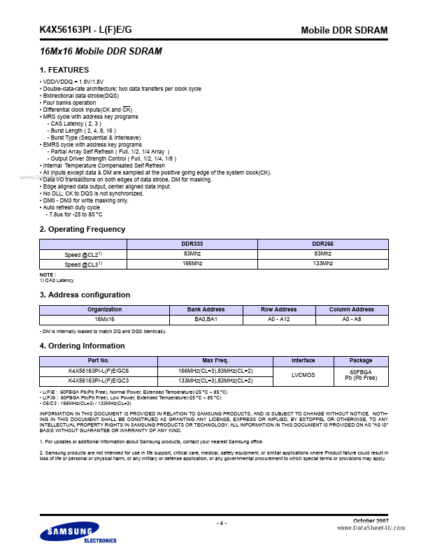
- VDD/VDDQ = 1.8V/1.8V
- Double-data-rate architecture; two data transfers per clock cycle
- Bidirectional data strobe(DQS)
- Four banks operation
- Differential clock inputs(CK and CK)
- MRS cycle with address key programs - CAS Latency ( 2, 3 ) - Burst Length ( 2, 4, 8, 16 ) - Burst Type (Sequential & Interleave)
- EMRS cycle with address key programs - Partial Array Self Refresh ( Full, 1/2, 1/4 Array ) - Output Driver Strength Control ( Full, 1/2, 1/4, 1/8 )
- Internal Temperature Compensated Self Refresh
- All inputs except data & DM are sampled at the positive going edge of the system clock(CK).
- Data I/O transactions on both edges of data strobe, DM for masking.