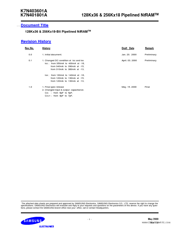
K7N401801A
K7N401801A is 128Kx36 & 256Kx18-Bit Pipelined NtRAMTM manufactured by Samsung Semiconductor.
DESCRIPTION
The K7N403601A and K7N401801A are 4,718,592 bits Synchronous Static SRAMs. The Nt RAMTM, or No Turnaround Random Access Memory utilizes all the bandwidth in any bination of operating cycles. Address, data inputs, and all control signals except output enable and linear burst order are synchronized to input clock. Burst order control must be tied "High or Low". Asynchronous inputs include the sleep mode enable(ZZ). Output Enable controls the outputs at any given time. Write cycles are internally self-timed and initiated by the rising edge of the clock input. This feature eliminates plex offchip write pulse generation and provides increased timing flexibility for inming signals. For read cycles, pipelined SRAM output data is temporarily stored by an edge trigered output register and then released to the output bufferes at the next rising edge of clock. The K7N403601A and K7N401801A are implemented with SAMSUNG′s high performance CMOS technology and is available in 100pin TQFP packages. Multiple power and ground pins minimize ground bounce.
FEATURES
- VDD=3.3V+0.165V/-0.165V Power Supply.
- VDDQ Supply Voltage 3.3V+0.165V/-0.165V for 3.3V I/O or 2.5V+0.4V/-0.125V for 2.5V I/O.
- Byte Writable Function.
- Enable clock and suspend operation.
- Single READ/WRITE control pin.
- Self-Timed Write Cycle.
- Three Chip Enable for simple depth expansion with no datacontention.
- Α interleaved burst or a linear burst mode.
- Asynchronous output enable control.
- Power Down mode.
- TTL-Level Three-State Outputs.
- 100-TQFP-1420A Package.
FAST ACCESS TIMES
PARAMETER Cycle Time Clock Access Time Output Enable Access Time Symbol t CYC t CD t OE -16 6.0 3.5 3.5 -15 6.7 3.8 3.8 -13 7.5 4.2 4.2 Unit ns ns ns
LOGIC BLOCK DIAGRAM
LBO A [0:16]or A [0:17] ADDRESS REGISTER A2~A16 or A2 ~A17 A0 ~A1
BURST ADDRESS...