K8D1716UTC
K8D1716UTC is 16M Bit (2M x8/1M x16) Dual Bank NOR Flash Memory manufactured by Samsung Semiconductor.
- Part of the K8D1716UBC comparator family.
- Part of the K8D1716UBC comparator family.
..
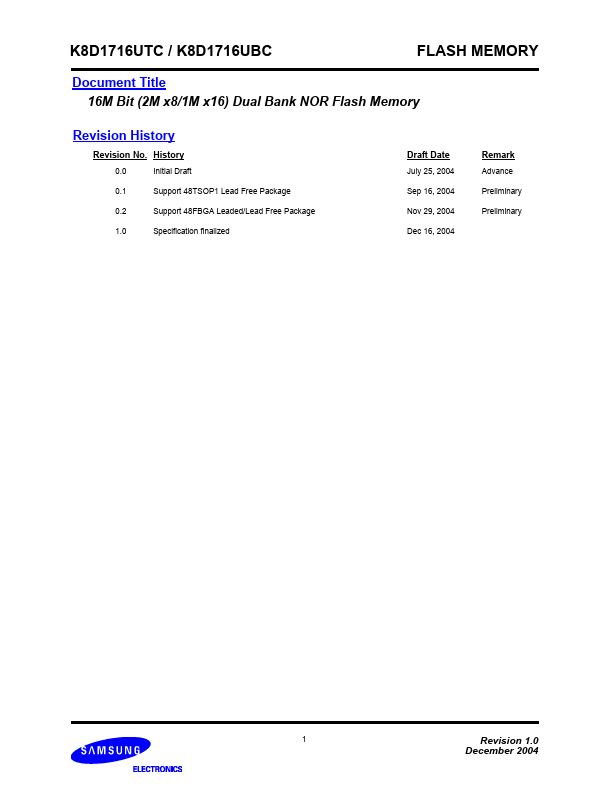
K8D1716UTC / K8D1716UBC
FLASH MEMORY
Document Title 16M Bit (2M x8/1M x16) Dual Bank NOR Flash Memory Revision History
Revision No. History
0.0 0.1 0.2 1.0 Initial Draft Support 48TSOP1 Lead Free Package Support 48FBGA Leaded/Lead Free Package Specification finalized
Draft Date
July 25, 2004 Sep 16, 2004 Nov 29, 2004 Dec 16, 2004
Remark
Advance Preliminary Preliminary
Revision 1.0 December 2004
K8D1716UTC / K8D1716UBC
16M Bit (2M x8/1M x16) Dual Bank NOR Flash Memory
Features
- Single Voltage, 2.7V to 3.6V for Read and Write operations
- Organization 1,048,576 x 16 bit (Word mode)
- Fast Read Access Time : 70ns
- Read While Program/Erase Operation
- Dual Bank...