KM4132G271A
KM4132G271A is 128K x 32Bit x 2 Banks Synchronous Graphic RAM manufactured by Samsung Semiconductor.
FEATURES
¡Ü ¡Ü
CMOS SGRAM
GENERAL DESCRIPTION
The KM4132G271A is 8,388,608 bits synchronous high data rate Dynamic RAM organized as 2 x 131,072 words by 32 bits, fabricated with SAMSUNG's high performance CMOS technology. Synchronous design allows precise cycle control with the use of system clock. I/O transactions are possible on every clock cycle. Range of operating frequencies, programmable burst length, and programmable latencies allows the same device to be useful for a variety of high bandwidth, high performance memory system applications. Write per bit and 8 columns block write improves performance in graphics systems.
¡Ü
¡Ü
¡Ü
¡Ü
¡Ü
¡Ü
¡Ü
¡Ü
JEDEC standard 3.3V power supply LVTTL patible with multiplexed address Dual bank / Pulse RAS MRS cycle with address key programs -. CAS Latency (2, 3) -. Burst Length (1, 2, 4, 8 & full page) -. Burst Type (Sequential & Interleave) All inputs are sampled at the positive going edge of the system clock Burst Read Single-bit Write operation DQM 0-3 for byte masking Auto & self refresh 16ms refresh period (1K cycle) 100 Pin QFP
ORDERING INFORMATION
Part NO. KM4132G271A-8 KM4132G271A-10 KM4132G271A-12 Cycle time 8ns 10ns 12ns Clock f 125MHz 100MHz 83MHz Access time@CL=3 7.0ns 7.0ns 9.0ns
Graphics Features
¡Ü
¡Ü
¡Ü
SMRS cycle. -. Load mask register -. Load color register Write Per Bit(Old Mask) Block Write(8 Columns)
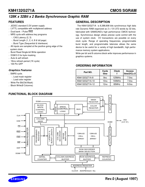
FUNCTIONAL BLOCK DIAGRAM
DQMi BLOCK WRITE CONTROL LOGIC CLK CKE CS COLUMN MASK DQMi DQi (i=0~31) MASK WRITE MASK REGISTER COLOR REGISTER INPUT BUFFER REFRESH COUNTER
CONTROL
LOGIC
TIMING REGISTER
SENSE AMPLIFIER
RAS CAS WE DSF DQMi
128Kx32 CELL ARRAY
128Kx32 CELL ARRAY
ROW DECORDER BANK SELECTION SERIAL COUNTER COLUMN ADDRESS BUFFER ROW ADDRESS BUFFER
ADDRESS REGISTER CLOCK ADDRESS(A 0~A9)
Rev.0 (August 1997)
OUTPUT BUFFER
LATENCY & BURST LENGTH
PROGRAMING REGISTER
COLUMN DECORDER
Reverse Type
Forward...