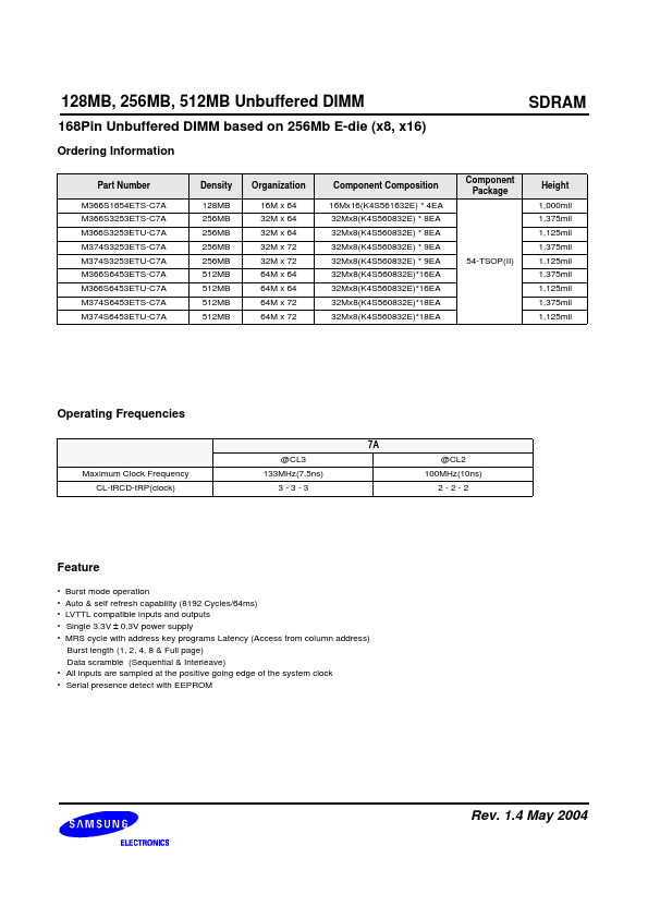
Datasheet4U Logo Datasheet4U.com

M366S1654ETS - SDRAM Unbuffered Module

Datasheet Summary

Description

Pin Name A0 ~ A12 BA0 ~ BA1 DQ0 ~ DQ63 CB0 ~ CB7 CLK0 ~ 3 CKE0, CKE1 CS0 ~ CS3 RAS CAS WE Select bank Data input/output Check bit (Data-in/data-out) Clock input Clock enable input Chip select input Row address strobe Colume address strobe Write enable Function Address input (Multiplexed) VDD VSS VRE

Features

  • 0 DQ1 DQ2 DQ3 DQ4 DQ5 DQ6 DQ7 CS U8 DQM DQ24 DQ25 DQ26 DQ27 DQ28 DQ29 DQ30 DQ31 DQ0 DQ1 DQ2 DQ3 DQ4 DQ5 DQ6 DQ7 CS U4 Serial PD SCL 47KΩ WP A0 SDA A1 A2 SA0 SA1 SA2 A0 ~ A12, BA0 & 1 RAS CAS WE CKE0 10Ω DQn VDD Vss.
  • SDRAM U0 ~ U8 SDRAM U0 ~ U8 SDRAM U0 ~ U8 SDRAM.

📥 Download Datasheet

Datasheet preview – M366S1654ETS

Datasheet Details

Part number M366S1654ETS
Manufacturer Samsung semiconductor
File Size 512.58 KB
Description SDRAM Unbuffered Module
Datasheet download datasheet M366S1654ETS Datasheet
Additional preview pages of the M366S1654ETS datasheet.
Other Datasheets by Samsung semiconductor

Full PDF Text Transcription

Click to expand full text
www.DataSheet4U.com 128MB, 256MB, 512MB Unbuffered DIMM SDRAM SDRAM Unbuffered Module 168pin Unbuffered Module based on 256Mb E-die 62/72-bit Non ECC/ECC Revision 1.4 May 2004 * Samsung Electronics reserves the right to change products or specification without notice. Rev. 1.4 May 2004 128MB, 256MB, 512MB Unbuffered DIMM Revision History Revision 1.0 (June, 2003) - First release Revision 1.1 (September, 2003) - Corrected Typo Revision 1.2 (February, 2004) - Corrected typo. Revision 1.3 (March. 2004) - Modified DC Characteristics Notes. Revision 1.4 (May, 2004) - Added Note 5. sentense of tRDL parameter SDRAM Rev. 1.
Published: |