LC35V1000BTS-70U Description
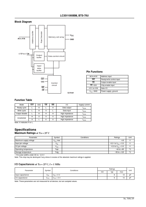
They provide two chip enable pins (CE1 and CE2) for device select/deselect control and one output enable pin (OE) for output control.
LC35V1000BTS-70U Key Features
- Low-voltage operation: 3.0 to 3.6 V
- Wide operating temperature range: -40 to +85°C
- Access time: 70 ns (maximum): LC35V1000BM and LC35V1000BTS-70U
- Low current drain Standby mode: 0.05 µA (typical-) at Ta = +25°C -: When VCC = 3.0 V 10.0 µA (maximum) at Ta = +70°C 20.
- Data retention voltage: 2.0 to 3.6 V
- No clock required (fully static circuits)
- Input/output shared function pins, 3-state output pins