2SA882
Overview
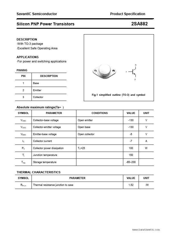
SavantIC Semiconductor Product Specification Silicon PNP Power Transistors 2SA882 DESCRIPTION ·With TO-3 package ·Excellent Safe Operating Area APPLICATIONS ·For power and switching applications ...
| Part | 2SA882 |
|---|---|
| Description | Silicon POwer Transistors |
| Category | Transistor |
| Manufacturer | SavantIC |
| Size | 134.64 KB |
SavantIC Semiconductor Product Specification Silicon PNP Power Transistors 2SA882 DESCRIPTION ·With TO-3 package ·Excellent Safe Operating Area APPLICATIONS ·For power and switching applications ...
| Part Number | Manufacturer | Description |
|---|---|---|
| 2SA882 | Inchange Semiconductor | POWER TRANSISTOR |
| 2SA886 | Panasonic | Silicon PNP epitaxial planar type Transistor |
| 2SA885 | Inchange Semiconductor | POWER TRANSISTOR |
| 2SA880 | Panasonic | SI PNP EPITAXIAL PLANAR TRANSISTOR |
| 2SA1560 | ROHM | Epitaxial Planar PNP Silicon Transistors |