2SC2791 Overview
Key Specifications
Description
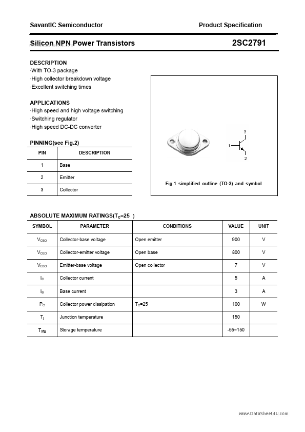
With TO-3 package - High collector breakdown voltage - Excellent switching times APPLICATIONS - High speed and high voltage switching - Switching regulator - High speed DC-DC converter PINNING(see Fig.2) PIN 1 2 3 Base Emitter DESCRIPTION 2SC2791 Fig.1 simplified outline (TO-3) and symbol Collector SYMBOL VCBO VCEO VEBO IC IB PC Tj Tstg PARAMETER Collector-base voltage Collector-emitter voltage Emitter-base voltage Collector current Base current Collector power dissipation Junction temperature Storage temperature TC=25 Open emitter Open base Open collector CONDITIONS VALUE 900 800 7 5 3 100 150 -55~150 UNIT V V V A A W SavantIC Semiconductor Product Specification Silicon NPN Power Transistors CHARACTERISTICS Tj=25 unless otherwise specified PARAMETER CONDITIONS MIN 2SC2791 SYMBOL TYP. MAX UNIT V(BR)CEO Collector-emitter breakdown voltage IC=10mA ;IB=0 800 V V(BR)CBO Collector-base breakdown voltage IC=1mA ;IE=0 900 V VCE(sat) VBE(sat) ICBO Collector-emitter saturation voltage IC=3A; IB=0.6A 1.0 V Base-emitter saturation voltage IC=3A; IB=0.6A 1.5 V Collector cut-off current VCB=800V; IE=0 100 µA IEBO Emitter cut-off current VEB=7V; IC=0 1 mA hFE-1 DC current gain IC=10mA ; VCE=5V 10 hFE-2 DC current gain IC=3A ; VCE=5V 10 Switching times tr tstg tf Rise time VCC=400V ,IC=3A, IB1=0.3A;IB2=-0.8A 1.0 µs Storage time 3.5 µs Fall time 1.0 µs 2 SavantIC Semiconductor Product Specification Silicon NPN Power Transistors PACKAGE OUTLINE 2SC2791 Fig.2 outline dimensions (unindicated tolerance:±0.1mm) 3.