2SC3043 Overview
Key Specifications
Max Operating Temp: 150 °C
Description
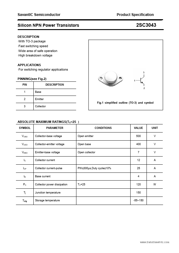
With TO-3 package - Fast switching speed - Wide area of safe operation - High breakdown voltage APPLICATIONS - For switching regulator applications PINNING(see Fig.2) PIN 1 2 3 Base Emitter DESCRIPTION 2SC3043 Fig.1 simplified outline (TO-3) and symbol Collector SYMBOL VCBO VCEO VEBO IC ICP IB PC Tj Tstg PARAMETER Collector-base voltage Collector-emitter voltage Emitter-base voltage Collector current Collector current-pulse Base current Collector power dissipation Junction temperature Storage temperature TC=25 PW ,300µs,Duty cycle,10% Open emitter Open base Open collector CONDITIONS VALUE 500 400 7 12 25 4 120 150 -55~150 UNIT V V V A A A W SavantIC Semiconductor Product Specification Silicon NPN Power Transistors CHARACTERISTICS Tj=25 unless otherwise specified PARAMETER Collector-emitter breakdown voltage Collector-base breakdown voltage Emitter-base breakdown voltage Collector-emitter saturation voltage Base-emitter saturation voltage Collector cut-off current Emitter cut-off current DC current gain DC current gain Transition frequency Output capacitance CONDITIONS IC=10mA ;RBE=< IC=1mA; IE=0 IE=1mA; IC=0 IC=8A; IB=1.6A IC=8A; IB=1.6A VCB=400V; IE=0 VEB=5V; IC=0 IC=1.6A ; VCE=5V IC=8A ; VCE=5V IC=1.6A ; VCE=10V IE=0; VCB=10V,f=1MHz 15 8 MIN 400 500 7 2SC3043 SYMBOL V(BR)CEO V(BR)CBO V(BR)EBO VCE(sat) VBE(sat) ICBO IEBO hFE-1 hFE-2 fT Cob TYP. MAX UNIT V V V 1.0 1.5 10 10 V V µA µA 20 160 MHz pF 2 SavantIC Semiconductor Product Specification Silicon NPN Power Transistors PACKAGE OUTLINE 2SC3043 Fig.2 outline dimensions (unindicated tolerance:±0.1mm) 3.