2SC3409 Overview
Description
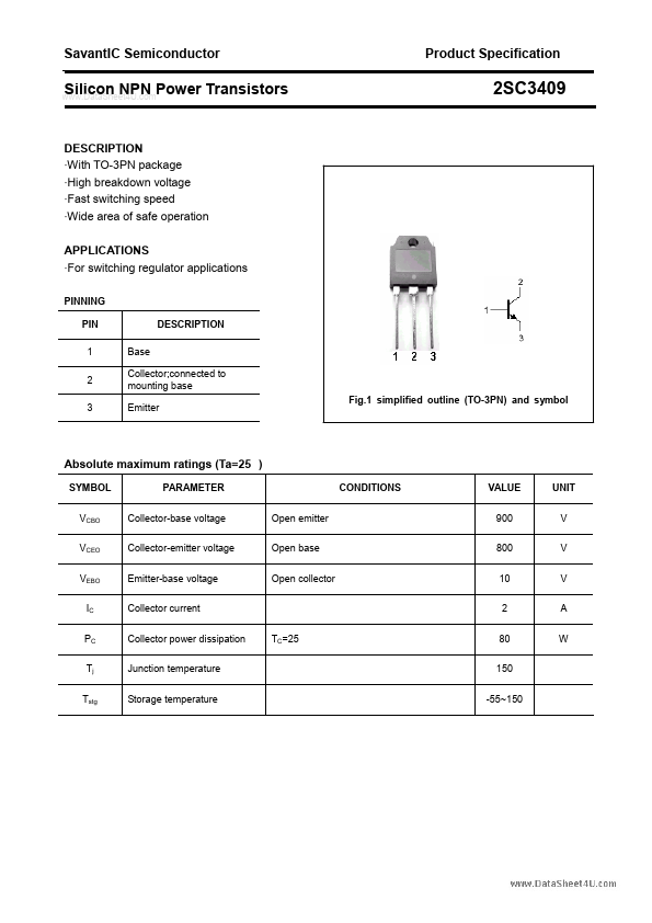
With TO-3PN package - High breakdown voltage - Fast switching speed - Wide area of safe operation APPLICATIONS - For switching regulator applications PINNING PIN 1 2 3 Base Collector;connected to mounting base Emitter Fig.1 simplified outline (TO-3PN) and symbol DESCRIPTION SYMBOL VCBO VCEO VEBO IC PC Tj Tstg PARAMETER Collector-base voltage Collector-emitter voltage Emitter-base voltage Collector current Collector power dissipation Junction temperature Storage temperature TC=25 Open emitter Open base Open collector CONDITIONS VALUE 900 800 10 2 80 150 -55~150 UNIT V V V A W SavantIC Semiconductor Product Specification Silicon NPN Power Transistors CHARACTERISTICS Tj=25 unless otherwise specified PARAMETER Collector-emitter breakdown voltage Collector-base breakdown voltage Emitter-base breakdown voltage Collector-emitter saturation voltage Base-emitter saturation voltage Collector cut-off current Emitter cut-off current DC current gain CONDITIONS IC=5mA ;RBE=7 IC=1mA ;IE=0 IE=1mA ;IC=0 IC=1.5A ;IB=0.3A IC=1.5A;IB=0.3A VCB=800V; IE=0 VEB=5V; IC=0 IC=0.5A ; VCE=4V 15 MIN 800 900 10 2SC3409 SYMBOL V(BR)CEO V(BR)CBO V(BR)EBO VCEsat VBEsat ICBO IEBO hFE TYP. MAX UNIT V V V 5.0 1.5 10 10 V V µA µA 2 SavantIC Semiconductor Product Specification Silicon NPN Power Transistors PACKAGE OUTLINE 2SC3409 Fig.2 outline dimensions 3.