BUX81 Overview
Description
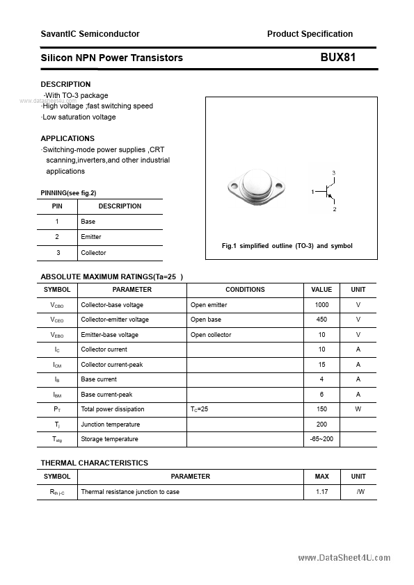
With TO-3 package - High voltage ;fast switching speed - Low saturation voltage APPLICATIONS - Switching-mode power supplies ,CRT scanning,inverters,and other industrial applications PINNING(see fig.2) PIN 1 2 3 Base Emitter Collector DESCRIPTION BUX81 Fig.1 simplified outline (TO-3) and symbol SYMBOL VCBO VCEO VEBO IC ICM IB IBM PT Tj Tstg PARAMETER Collector-base voltage Collector-emitter voltage Emitter-base voltage Collector current Collector current-peak Base current Base current-peak Total power dissipation Junction temperature Storage temperature TC=25 CONDITIONS Open emitter Open base Open collector VALUE 1000 450 10 10 15 4 6 150 200 -65~200 UNIT V V V A A A A W SYMBOL Rth j-C PARAMETER SavantIC Semiconductor Product Specification Silicon NPN Power Transistors CHARACTERISTICS Tj=25 unless otherwise specified PARAMETER Collector-emitter sustaining voltage Collector-emitter saturation voltage Collector-emitter saturation voltage Base-emitter saturation voltage Base-emitter saturation voltage Collector cut-off current Emitter cut-off current DC current gain Transition frequency Output capacitance CONDITIONS IC=0.1A; L=25mH IC=5 A;IB=1 A IC=8 A;IB=2.5 A IC=5 A;IB=1 A IC=8 A;IB=2.5 A VCE=1000V;VBE=0 TC=125 VEB=10V; IC=0 IC=1.2A ; VCE=5V IC=0.5A ; VCE=10V IE=0 ; VCB=20V;f=0.1MHz 20 8 105 MIN 450 BUX81 SYMBOL VCEO(SUS) VCEsat-1 VCEsat-2 VBEsat-1 VBEsat-2 ICES IEBO hFE fT COB TYP. MAX UNIT V 1.5 3.0 1.4 1.8 1.0 3.0 10 V V V V mA mA MHz pF Switching times ton ts tf Turn-on time Storage time Fall time IC=5A ;IB1=1A; IB2=-2A VCC=250V 0.5 3.5 0.8 µs µs µs 2 SavantIC Semiconductor Product Specification Silicon NPN Power Transistors PACKAGE OUTLINE BUX81 Fig.2 Outline dimensions 3.