MJ16012 Overview
Description
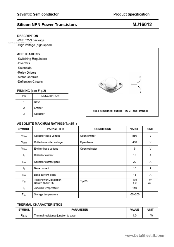
With TO-3 package - High voltage ,high speed APPLICATIONS - Switching Regulators - Inverters - Solenoids - Relay Drivers - Motor Controls - Deflection Circuits PINNING (see Fig.2) PIN 1 2 3 Base Emitter Collector DESCRIPTION MJ16012 Fig.1 simplified outline (TO-3) and symbol SYMBOL VCBO VCEO VEBO IC ICM IB IBM PD Ti Tstg PARAMETER Collector-base voltage Collector-emitter voltage Emitter-base voltage Collector current Collector current-peak Base current Base current-peak Total Power Dissipation Derate above 25 Junction temperature Storage temperature TC=25 CONDITIONS Open emitter Open base Open collector VALUE 850 450 6 15 20 10 15 175 1.0 150 -65~200 UNIT V V V A A A A W W/ SYMBOL Rth j-c PARAMETER SavantIC Semiconductor Product Specification Silicon NPN Power Transistors CHARACTERISTICS Tj=25 unless otherwise specified PARAMETER Collector-emitter sustaining voltage Collector-emitter saturation voltage Collector-emitter saturation voltage Base-emitter saturation voltage Collector cut-off current Collector cut-off current Emitter cut-off current DC current gain Output capacitance CONDITIONS IC=0.1A ;IB=0 IC=5A; IB=0.5A IC=10A ;IB=1.0A TC=100 IC=10A ;IB=1.0A TC=100 VCE=850V;RBE=50>;TC=100 VCE=850V; VBE(off)=1.5V TC=100 VEB=6V; IC=0 IC=15A ; VCE=5V VCB=10V,IE=0;f=1.0KHz 7 MIN 450 MJ16012 SYMBOL VCEO(SUS) VCE(sat)-1 VCE(sat)-2 VBE(sat) ICER ICEV IEBO hFE COB TYP. MAX UNIT V 2.5 3.0 3.0 1.5 1.5 2.5 0.25 1.5 10 V V V mA mA mA 400 pF Switching times resistive load td tr ts tf Delay time Rise time Storage time Fall time IC=10A ; VCC=250V IB1=1.0A ;IB2=2.0A PW=30µs; RB2=1.6> Duty CycleD2.0% 20 200 900 150 ns ns ns ns 2 SavantIC Semiconductor Product Specification Silicon NPN Power Transistors PACKAGE OUTLINE.