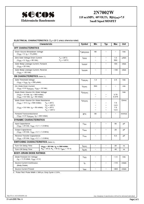
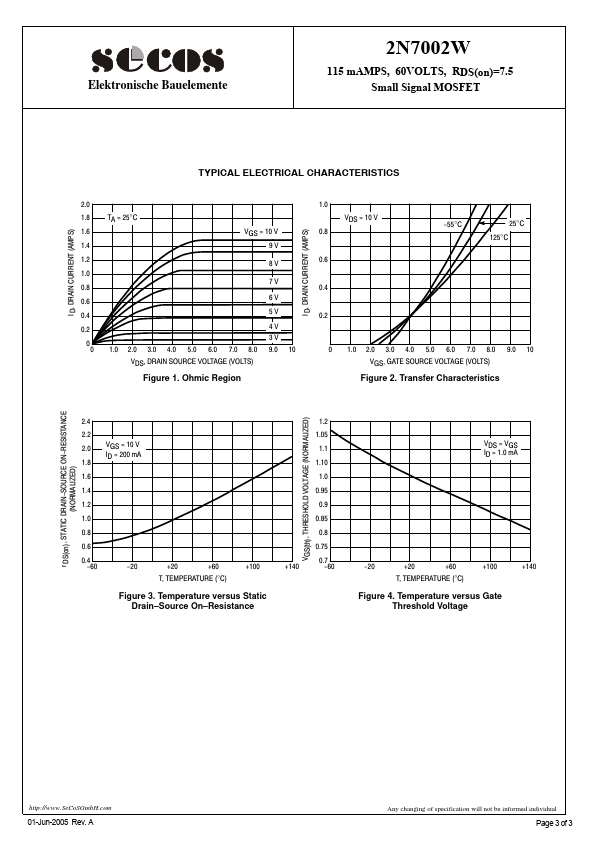
SeCoS Halbleitertechnologie GmbH 2N7002W
Small Signal MOSFET
| Part No. | 2N7002W |
|---|---|
| Datasheet | 2N7002W Download |
| Manufacturer |  SeCoS Halbleitertechnologie GmbH |
| Description | Small Signal MOSFET |
| Buy | Stock & Price |
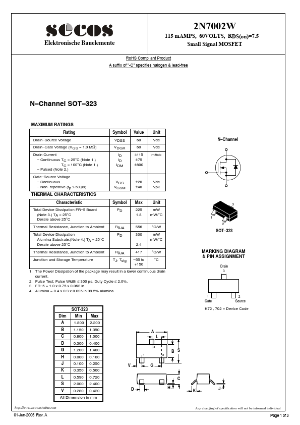
MAXIMUM RATINGS
Rating Symbol Value Unit Drain–Source Voltage Drain–Gate Voltage (RGS = 1.0 MΩ) Drain Current – Continuous TC = 25°C (Note 1.) – Continuous TC = 100°C (Note 1.) – Pulsed (Note 2.) VDSS VDGR ID ID IDM 60 60 ±ā115 ±ā75 ±ā800 Vdc Vdc mAdc Gate–Source Voltage – Continuous – Non–repetitive (tp ≤ 50 µs) THERMAL CHARACTERISTICS VGS ±ā20 Vdc VGSM ±ā40 Vpk Characteristic Symbol Max Unit Total Device Dissipation FR–5 Board (Note 3.) TA = 25°C Derate above 25°C PD 225 mW 1.8 mW/°C Thermal Resistance, Junction to Ambient Total Device Dissipation Alumina Substrate,(Note 4.) TA = 25°C Derate above 25°C RθJA PD 556 °C/W 300 mW mW/°C 2.4 Thermal Resistance, Junction to Ambient Junction and Storage Temperature RθJA TJ, Tstg 417 –ā55 to +150 °C/W °C 1. The Power Dissipation of the package may result in a lower continuous drain current. 2. Pulse Test: Pulse Width ≤ 300 µs, Duty Cycle ≤ 2.0%. 3. FR–5 = 1.0 x 0.75 x 0.062 in. 4. Alumina = 0.4 x 0.3 x 0.025 in 99.5% alumina. SOT-323 Dim Min...