2N7002W
Key Features
- Low On-Resistance
- Low Gate Threshold Voltage
- Low Input Capacitance
- Fast Switching Speed
- Low Input/Output Leakage
- Ultra-Small Surface Mount Package
- Lead Free/RoHS Compliant
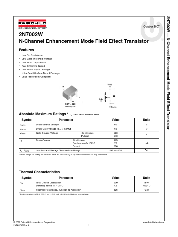
- G SOT - 323 Marking : 2N S
| Part Number | Manufacturer | Description |
|---|---|---|
| 2N7002W | Galaxy Microelectronics | N-Channel Power Mosfet |
| 2N7002W | JCET | N-Channel MOSFET |
| 2N7002W | Weitron Technology | N-Channel MOSFET |
| 2N7002W | Kexin Semiconductor | N-Channel MOSFET |
| 2N7002W | SeCoS Halbleitertechnologie GmbH | Small Signal MOSFET |
| 2N7002W | onsemi | Small Signal MOSFET |
| 2N7002W-G | Comchip Technology | MOSFET |
| 2N7002W | Galaxy Microelectronics | N-channel MOSFET |
| 2N7002W | Diodes Incorporated | N-Channel MOSFET |
| 2N7002W | Micro Commercial Components | N-channel MOSFET |