2N7002MTF
Key Features
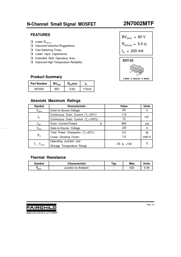
- Source
- Drain
| Part Number | Manufacturer | Description |
|---|---|---|
| 2N7002M | Jiangsu Changjiang Electronics | MOSFET |
| 2N7002KB | Silikron Semiconductor | MOSFET |
| 2N7002CSM | Seme LAB | N-channel MOSFET |
| 2N7002DW | Diodes Incorporated | DUAL N-CHANNEL MOSFET |
| 2N7002L | onsemi | N-Channel MOSFET |
| 2N7002W | Galaxy Microelectronics | N-Channel Power Mosfet |
| 2N7002W | JCET | N-Channel MOSFET |
| 2N7002E | onsemi | Small Signal MOSFET |
| 2N7002DW | Weitron Technology | Dual N-Channel MOSFET |
| 2N7002VA | Diodes Incorporated | DUAL N-CHANNEL ENHANCEMENT MODE FIELD EFFECT TRANSISTOR |