IRF450
IRF450 is N-Channel Power MOSFET manufactured by Seme LAB.
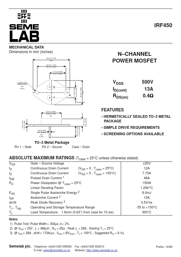
FEATURES
500V 13A 0.4W
20.32 (0.800) 18.80 (0.740) dia. 1.78 (0.070) 1.52 (0.060) 7.87 (0.310) 6.99 (0.275)
- HERMETICALLY SEALED TO- 3 METAL PACKAGE
- SIMPLE DRIVE REQUIREMENTS
- SCREENING OPTIONS AVAILABLE
1.09 (0.043) 0.97 (0.038) dia. 2 plcs.
TO- 3 Metal Package
Pin 1
- Gate Pin 2
- Source Case
- Drain
ABSOLUTE MAXIMUM RATINGS (Tcase = 25°C unless otherwise stated)
VGS ID ID IDM PD EAS IAR dv/dt TJ , Tstg TL Gate
- Source Voltage Continuous Drain Current (VGS = 0 , Tcase = 25°C) Continuous Drain Current (VGS = 0 , Tcase = 100°C) Pulsed Drain Current 1 Power Dissipation @ Tcase = 25°C Linear Derating Factor Single Pulse Avalanche Energy 2 Avalanche Current 2 Peak Diode Recovery 3 Operating and Storage Temperature Range Lead Temperature 1.6mm (0.63”) from case for 10 sec. ±20V 12A 7.75A 48A 150W 1.2W/°C 8.0m J 12A 3.5V/ns -55 to +150°C 300°C
Notes 1) Pulse Test: Pulse Width £ 300ms, d £ 2% 2) @ VDD = 25V , L ³ 480m H , RG = 25W , Peak IL = 28A , Starting TJ = 25°C 3) @ ISD £ 28A , di/dt £ 170A/ms , VDD £ BVDSS , TJ £ 150°C , Suggested RG = 9.1W
Semelab plc.
Telephone +44(0)1455 556565. Fax +44(0)1455 552612. Website: http://.semelab.co.uk E-mail: sales@semelab.co.uk
12.07 (0.475) 11.30 (0.445)
Prelim. 10/99
ELECTRICAL CHARACTERISTICS (Tcase = 25°C unless otherwise stated)
Parameter
STATIC ELECTRICAL RATINGS BVDSS Drain
- Source Breakdown Voltage DBVDSS Temperature Coefficient of DTJ Breakdown Voltage Static Drain
- Source On- State RDS(on) Resistance 1 VGS(th) Gate Threshold Voltage gfs Forward Transconductance 1 IDSS IGSS IGSS Ciss Coss Crss Qg Qgs Qgd td(on) tr td(off) tf IS ISM VSD trr Qrr ton LD LS Zero Gate Voltage Drain Current Forward Gate
- Source Leakage Reverse Gate
- Source Leakage DYNAMIC CHARACTERISTICS Input Capacitance Output Capacitance Reverse Transfer Capacitance Total Gate Charge Gate
- Source Charge Gate
- Drain (“Miller”) Charge Turn- On Delay Time Rise Time Turn- Off Delay Time Fall Time
Test Conditions
VGS = 0 ID = 1m A...