LH28F004SU-Z1
LH28F004SU-Z1 is 4M (512K bb 8) Flash Memory manufactured by Sharp Corporation.
Features
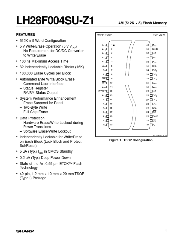
40-PIN TSOP
4M (512K × 8) Flash Memory
TOP VIEW
- 512K × 8 Word Configuration
- 5 V Write/Erase Operation (5 V VPP)
- No Requirement for DC/DC Converter to Write/Erase
A16 A15 A14 A13 A12 A11 A9 A8 WE RP VPP RY/BY A18 A7 A6 A5 A4 A3 A2 A1
1 2 3 4 5 6 7 8 9 10 11 12 13 14 15 16 17 18 19 20
40 39 38 37 36 35 34 33 32 31 30 29 28 27 26 25 24 23 22 21
A17 GND NC NC A10 DQ7 DQ6 DQ5 DQ4 VCC VCC NC DQ3 DQ2 DQ1 DQ0 OE GND CE A0
- -
- -
100 ns Maximum Access Time 32 Independently Lockable Blocks (16K) 100,000 Erase Cycles per Block Automated Byte Write/Block Erase
- mand User Interface
- Status Register » BY » Status Output
- RY /
- Erase Suspend for Read
-...