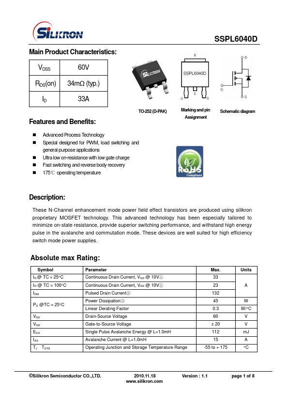
SSPL6040D
SSPL6040D is N-Channel enhancement mode power field effect transistors manufactured by Silikron Semiconductor.
Features and Benefits:
TO-252 (D-PAK)
- Advanced Process Technology
- Special designed for PWM, load switching and general purpose applications
- Ultra low on-resistance with low gate charge
- Fast switching and reverse body recovery
- 175℃ operating temperature
Marking and pin Assignment
Schematic diagram
Description
:
These N-Channel enhancement mode power field effect transistors are produced using silikron proprietary MOSFET technology. This advanced technology has been especially tailored to minimize on-state resistance, provide superior switching performance, and withstand high energy pulse in the avalanche and mutation mode. These devices are well suited for high efficiency switch mode power supplies.
Absolute max Rating:
Symbol ID @ TC = 25°C ID @ TC = 100°C IDM
PD @TC = 25°C
VDS VGS EAS IAS TJ TSTG
Parameter Continuous Drain Current, VGS @ 10V① Continuous Drain Current, VGS @ 10V① Pulsed Drain Current② Power Dissipation③ Linear Derating Factor Drain-Source Voltage Gate-to-Source Voltage Single Pulse Avalanche Energy @ L=1.0m H Avalanche Current @ L=1.0m H Operating Junction and Storage Temperature Range
Max. 33 23 132 45 0.3 60 ± 20 112 15
-55 to + 175
Units
W W/°C
V V m J A °C
©Silikron Semiconductor CO.,LTD.
2010.11.18 .silikron.
Version : 1.1 page 1 of 8
Thermal Resistance
Symbol RθJC RθJA
Characterizes Junction-to-case③ Junction-to-ambient (t ≤ 10s) ④
Typ.
- -
Electrical Characterizes @TA=25℃ unless otherwise specified
Symbol Parameter V(BR)DSS Drain-to-Source breakdown voltage
RDS(on) Static Drain-to-Source on-resistance
VGS(th) Gate threshold voltage
IDSS Drain-to-Source leakage current
IGSS Gate-to-Source forward leakage
Qg Total gate charge
Qgs Gate-to-Source charge
Qgd Gate-to-Drain("Miller") charge...