Datasheet Summary
SSM9926A man Drain Dual N-Channel Enhancement Mode MOSFET
Product Summary
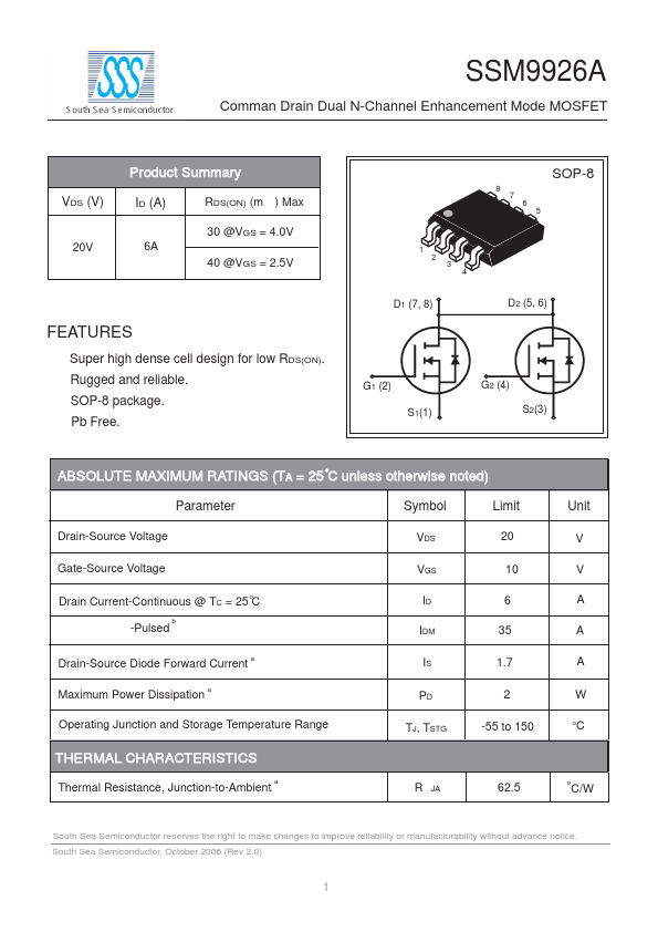
SOP-8
7 6 5
VDS (V)
ID (A)
RDS(ON) (m ) Max 30 @VGS = 4.0V
20V
6A 40 @VGS = 2.5V
3 4
D1 (7, 8)
D2 (5, 6)
Features
Super high dense cell design for low RDS(ON). Rugged and reliable. SOP-8 package. Pb Free.
S1(1) G1 (2) G2 (4)...