2N7079
Overview
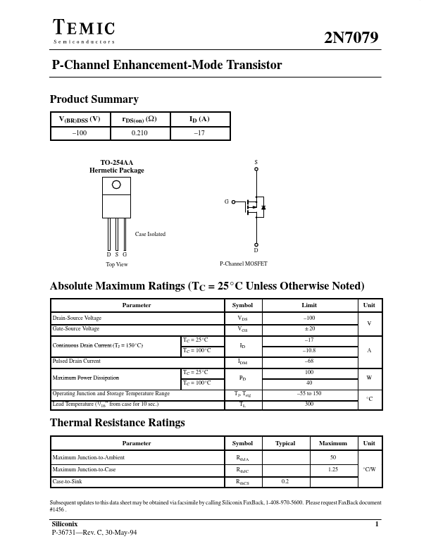
P-Channel Enhancement-Mode Transistor Product Summary V(BR)DSS (V) –100 rDS(on) (W) 0.210 ID (A) –17 TO-254AA S Hermetic Package 2N7079 G Case Isolated DSG Top View D P-Channel MOSFET Abso...
| Part | 2N7079 |
|---|---|
| Description | P-Channel Transistor |
| Category | Transistor |
| Manufacturer | TEMIC Semiconductors |
| Size | 118.28 KB |
P-Channel Enhancement-Mode Transistor Product Summary V(BR)DSS (V) –100 rDS(on) (W) 0.210 ID (A) –17 TO-254AA S Hermetic Package 2N7079 G Case Isolated DSG Top View D P-Channel MOSFET Abso...
| Part Number | Manufacturer | Description |
|---|---|---|
| 2N7076 | Inchange Semiconductor | N-Channel MOSFET |