Si9405DY
Si9405DY is P-Channel Enhancement-Mode MOSFET manufactured by TEMIC Semiconductors.
P-Channel Enhancement-Mode MOSFET
Product Summary
VDS (V)
- 20 r DS(on) (W)
0.10 @ VGS =
- 10 V 0.16 @ VGS =
- 4.5 V
ID (A)
"4.3 "3.4
Remended upgrade: Si9430DY Lower profile/smaller size- see LITE FOOTR equivalent: Si6447DQ
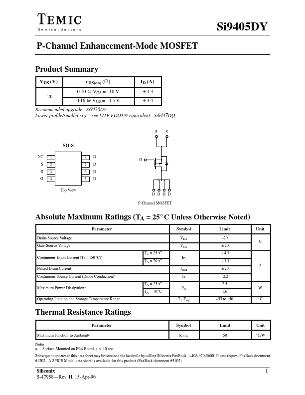
SO-8
NC S S G 1 2 3 4 Top View D D D D P-Channel MOSFET 8 7 6 5 D D D D G
Absolute Maximum Ratings (TA = 25_C Unless Otherwise Noted)
Parameter
Drain-Source Voltage Gate-Source Voltage Continuous Drain Current (TJ = 150_C)a Pulsed Drain Current Continuous Source Current (Diode Conduction)a Maximum Power Dissipationa Operating Junction and Storage Temperature Range TA = 25_C TA = 70_C TA = 25_C TA = 70_C
Symbol
VDS VGS ID IDM IS PD TJ, Tstg
Limit
- 20 "20 "4.3 "3.3 "20
- 2.2 2.5 1.6
- 55 to 150
Unit
W _C
Thermal Resistance Ratings
Parameter
Maximum Junction-to-Ambienta Notes a. Surface Mounted on FR4 Board, t v 10 sec. Subsequent updates to this data sheet may be obtained via facsimile by calling Siliconix Fax Back, 1-408-970-5600. Please request Fax Back document #1202. A SPICE Model data sheet is available for this product (Fax Back document #5102).
Symbol
Rth JA
Limit
Unit
_C/W
Siliconix S-47958- Rev. H, 15-Apr-96
Specifications (TJ = 25_C Unless Otherwise Noted)
Parameter Static
Gate Threshold Voltage Gate-Body Leakage Zero Gate Voltage Drain Current VGS(th) IGSS IDSS VDS = VGS, ID =
- 250 m A VDS = 0 V, VGS = "20 V VDS...