THC63LVD104S
THC63LVD104S is 112MHz 30Bits Color LVDS Receiver manufactured by THine Electronics.
Description
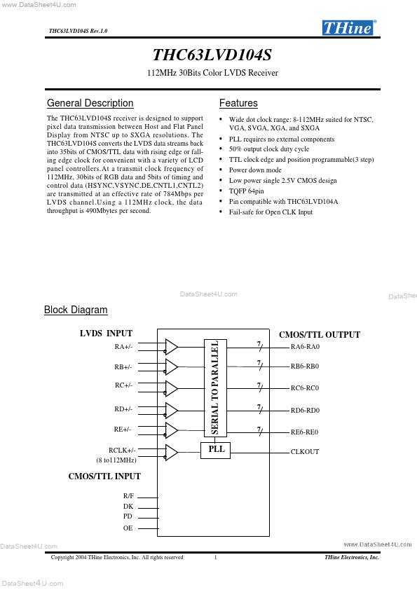
The THC63LVD104S receiver is designed to support pixel data transmission between Host and Flat Panel Display from NTSC up to SXGA resolutions. The THC63LVD104S converts the LVDS data streams back into 35bits of CMOS/TTL data with rising edge or falling edge clock for convenient with a variety of LCD panel controllers.At a transmit clock frequency of 112MHz, 30bits of RGB data and 5bits of timing and control data (HSYNC,VSYNC,DE,CNTL1,CNTL2) are transmitted at an effective rate of 784Mbps per LVDS channel.Using a 112MHz clock, the data throughput is 490Mbytes per second.
Features
- Wide dot clock range: 8-112MHz suited for NTSC,
VGA, SVGA, XGA, and SXGA
- -
- -
- -
- -
PLL requires no external ponents 50% output clock duty cycle TTL clock edge and position programmable(3 step) Power down mode Low power single 2.5V CMOS design TQFP 64pin Pin patible with THC63LVD104A Fail-safe for Open CLK Input
.
Data Shee
Block Diagram
LVDS INPUT SERIAL TO PARALLEL
RA+/RB+/RC+/7 7 7 7 7
CMOS/TTL OUTPUT
RA6-RA0 RB6-RB0 RC6-RC0 RD6-RD0 RE6-RE0 CLKOUT
RD+/RE+/RCLK+/(8 to112MHz)
CMOS/TTL INPUT
R/F DK PD OE
.
Copyright 2004 THine Electronics, Inc. All rights reserved 1 THine Electronics, Inc.
Data Sheet 4 U .
..
THC63LVD104S Rev.1.0
Pin Out et4U.
RARA+ RBRB+ LVCC RCRC+ RCLKRCLK+ LGND RDRD+ RERE+ PGND PVCC
48 47 46 45 44 43 42 41 40 39 38 37 36 35 34 33
VCC RA0 RA1 RA2 GND RA3 RA4 RA5 RA6 RB0 RB1 VCC RB2 RB3 RB4 RB5
49 50 51 52 53 54 55 56 57 58 59 60 61 62 63 64
.
32 31 30 29 28 27 26 25 24 23 22 21 20 19 18 17
RB6 CLKOUT GND RC0 RC1 RC2 RC3 RC4 RC5 VCC RC6 RD0 RD1 RD2 RD3 RD4
Data Shee
.
Copyright 2004 THine Electronics, Inc. All rights reserved 2 THine Electronics, Inc.
Data Sheet 4 U .
GND DK PD OE R/F RE6 RE5 RE4 VCC RE3 RE2 RE1 RE0 RD6 RD5 GND
1 2 3 4 5 6 7 8 9 10 11 12 13 14 15...