TSM2N7002E Overview
Key Features
- 3 4 2.5 1.0 ± 100
| Part | TSM2N7002E |
|---|---|
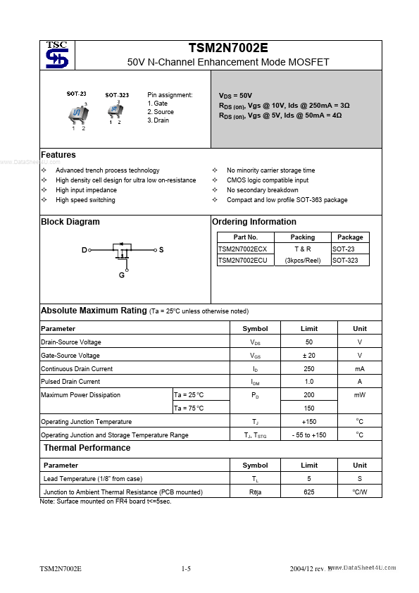
| Description | 50V N-Channel Enhancement Mode MOSFET |
| Category | MOSFET |
| Manufacturer | Taiwan Semiconductor |
| Size | 234.54 KB |
| Part Number | Manufacturer | Description |
|---|---|---|
| TSM2N7002KD | Taiwan Semiconductor | 60V N-Channel MOSFET |
| M2N7000 | Taiwan Semiconductor | TSM2N7000 |