TSM20N50CN
TSM20N50CN is 500V N-Channel Power MOSFET manufactured by Taiwan Semiconductor.
500V N-Channel Power MOSFET
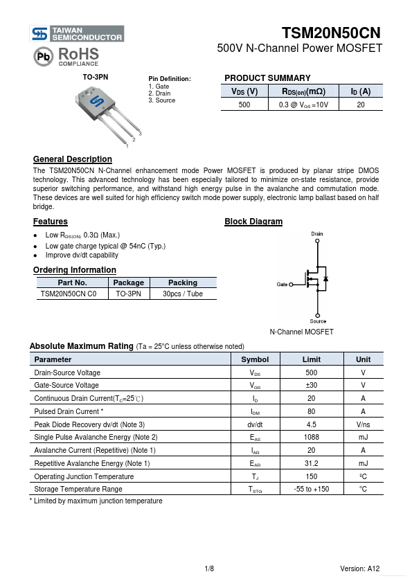
TO-3PN
Pin Definition: 1. Gate 2. Drain 3. Source
PRODUCT SUMMARY VDS (V)
RDS(on)(mΩ)
0.3 @ VGS =10V
ID (A)
General Description
The TSM20N50CN N-Channel enhancement mode Power MOSFET is produced by planar stripe DMOS technology. This advanced technology has been especially tailored to minimize on-state resistance, provide superior switching performance, and withstand high energy pulse in the avalanche and mutation mode. These devices are well suited for high efficiency switch mode power supply, electronic lamp ballast based on half bridge.
Features
- -
- Low RDS(ON) 0.3Ω (Max.) Low gate charge typical @ 54nC (Typ.) Improve dv/dt...