Techcode TDM3421
The TDM3421 uses advanced trench technology to provide excellent RDS(ON) and low gate charge. This device is suitable for use as a load switch or in PWM applications.| Part No. | TDM3421 |
|---|---|
| Datasheet | TDM3421 Download |
| Manufacturer |  Techcode |
| Description | P-Channel Enhancement Mode MOSFET |
| Buy | Stock & Price |
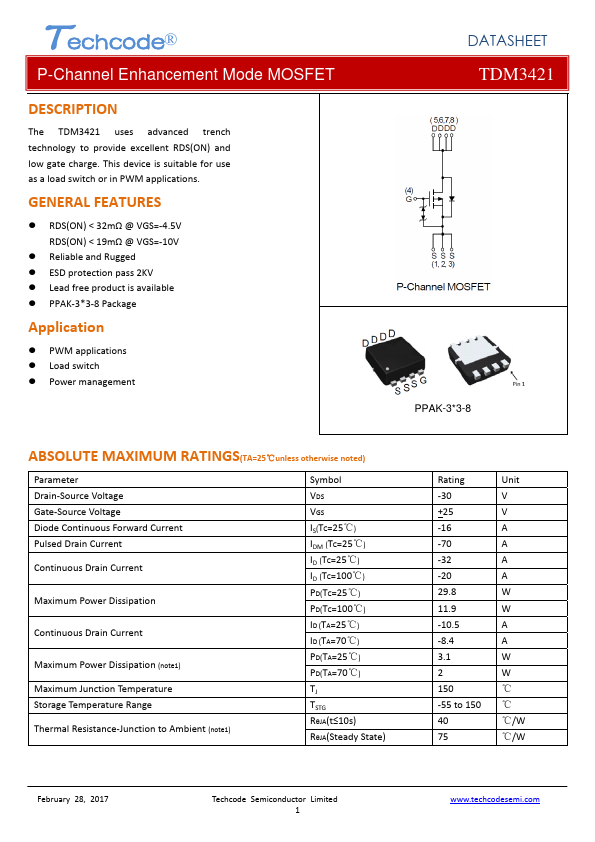
DESCRIPTION
GENERAL FEATURES
● RDS(ON) < 32mΩ @ VGS=‐4.5V RDS(ON) < 19mΩ @ VGS=‐10V● Reliable and Rugged
● ESD protection pass 2KV
● Lead free product is available
● PPAK‐3*3‐8 Package Application
● PWM applications
● Load switch
● Power management
ABSOLUTE MAXIMUM RATINGS
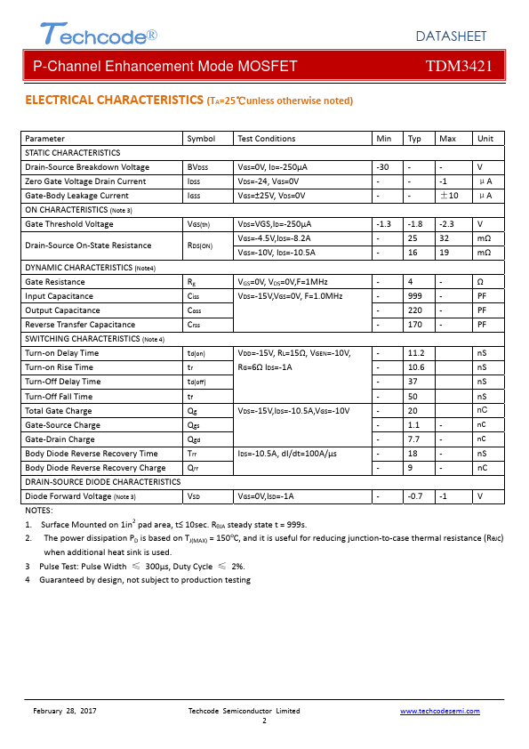
(TA=25℃unless otherwise noted) Parameter Drain‐Source Voltage Gate‐Source Voltage Diode Continuous Forward Current Pulsed Drain Current Continuous Drain Current Maximum Power Dissipation Continuous Drain Current Maximum Power Dissipation (note1) Maximum Junction Temperature Storage Temperature Range Thermal Resistance‐Junction to Ambient (note1) Symbol VDS VGS IS(TC=25℃) IDM (TC=25℃) ID (TC=25℃) ID (TC=100℃) PD(TC=25℃) PD(TC=100℃) ID (TA=25℃) ID (TA=70℃) PD(TA=25℃) PD(TA=70℃) TJ TSTG RθJA(t≤10s) RθJA(Steady State) DATASHEET TDM3421 PPAK-3*3-8 Rating ‐30 +25 ‐16 ‐70 ‐32 ‐20 29.8 11.9 ‐10.5 ‐8.4 3.1 2 150 ‐55 to 150 40 75 Unit V V A A A A W W A A W W ℃ ℃ ℃/W ℃/W February 28, 2017 Techcode Semiconductor Limited 1 T echc...