Datasheet4U Logo Datasheet4U.com

2SJ315 - P-Channel MOSFET

Key Features

  • z 4.
  • Volt gate drive z Low drain.
  • source ON resistance : RDS (ON) = 0.25 Ω (typ. ) z High forward transfer admittance : |Yfs| = 3.0 S (typ. ) z Low leakage current : IDSS =.
  • 100 µA (max) (VDS =.
  • 60 V) z Enhancement mode : Vth =.
  • 0.8~.
  • 2.0 V (VDS =.
  • 10 V, ID =.
  • 1 mA) Absolute Maximum Ratings (Ta = 25°C) Characteristics Symbol Rating Unit Drain.
  • source voltage Drain.
  • gate voltage (RGS = 20 kΩ) Gate.
  • source volt.

📥 Download Datasheet

Datasheet Details

Part number 2SJ315
Manufacturer Toshiba
File Size 219.28 KB
Description P-Channel MOSFET
Datasheet download datasheet 2SJ315 Datasheet

Full PDF Text Transcription (Reference)

The following content is an automatically extracted verbatim text from the original manufacturer datasheet and is provided for reference purposes only.

View original datasheet text
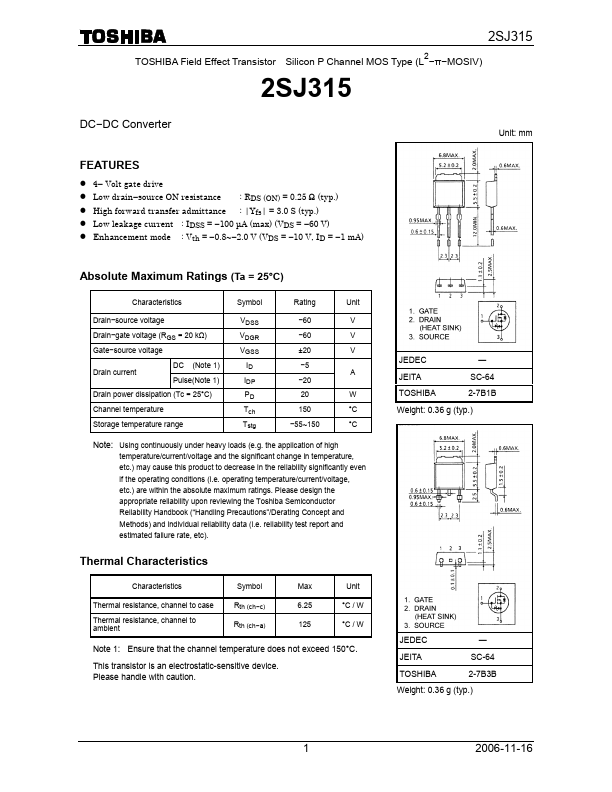
2SJ315 TOSHIBA Field Effect Transistor Silicon P Channel MOS Type (L2−π−MOSIV) 2SJ315 DC−DC Converter Unit: mm FEATURES z 4− Volt gate drive z Low drain−source ON resistance : RDS (ON) = 0.25 Ω (typ.) z High forward transfer admittance : |Yfs| = 3.0 S (typ.) z Low leakage current : IDSS = −100 µA (max) (VDS = −60 V) z Enhancement mode : Vth = −0.8~−2.0 V (VDS = −10 V, ID = −1 mA) Absolute Maximum Ratings (Ta = 25°C) Characteristics Symbol Rating Unit Drain−source voltage Drain−gate voltage (RGS = 20 kΩ) Gate−source voltage Drain current DC (Note 1) Pulse(Note 1) Drain power dissipation (Tc = 25°C) Channel temperature Storage temperature range VDSS VDGR VGSS ID IDP PD Tch Tstg −60 −60 ±20 −5 −20 20 150 −55~150 V V V A W °C °C Note: Using continuously under heavy loads (e.