Datasheet Summary
MOSFETs Silicon N-Channel MOS (π-MOS)
TK13A25D
1. Applications
- Switching Voltage Regulators
2. Features
(1) Low drain-source on-resistance: RDS(ON) = 0.19 Ω (typ.) (2) Low leakage current: IDSS = 10 µA (max) (VDS = 250 V) (3) Enhancement mode: Vth = 1.5 to 3.5 V (VDS = 10 V, ID = 1 mA)
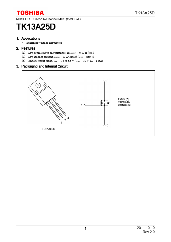
3. Packaging and Internal Circuit
TK13A25D
TO-220SIS
1: Gate (G) 2: Drain (D) 3: Source (S)
1 2011-10-10 Rev.2.0
TK13A25D
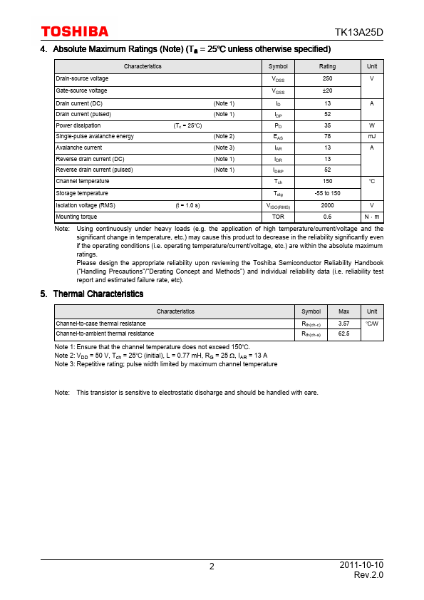
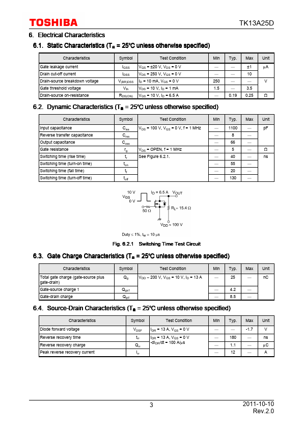
4....