Datasheet4U Logo Datasheet4U.com

K15J50D - TK15J50D

📥 Download Datasheet

Full PDF Text Transcription (Reference)

The following content is an automatically extracted verbatim text from the original manufacturer datasheet and is provided for reference purposes only.

View original datasheet text
TK15J50D TOSHIBA Field Effect Transistor Silicon N Channel MOS Type (π-MOSⅦ) TK15J50D Switching Regulator Applications
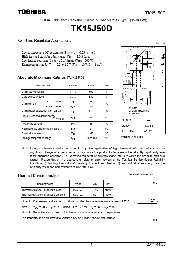
 15.9 MAX. Unit: mm Ф3.2 ± 0.2 1.0 4.5 9.0 2.0 3.3 MAX. 2.0 Absolute Maximum Ratings (Ta = 25°C) Characteristics Drain-source voltage Gate-source voltage Drain current DC Pulse (Note 1) (Note 1) Symbol VDSS VGSS ID IDP PD EAS IAR EAR Tch Tstg Rating 500 ±30 15 60 210 360 15 21 150 −55 to 150 Unit 2.0 ± 0.3 1.0 +0.3 -0.25 5.45 ± 0.2 1.8 MAX. +0.3 0.6 -0.1 5.45 ± 0.2 4.8 MAX. V V A W mJ A mJ °C °C Drain power dissipation (Tc = 25°C) Single pulse avalanche energy (Note 2) Avalanche current Repetitive avalanche energy (Note 3) Channel temperature Storage temperature range 1: Gate 2: Drain (Heatsink) 3: Source 2.