SSM3K119TU Overview
Key Features
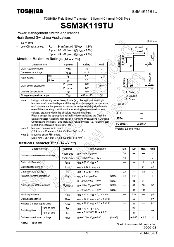
- Low ON-resistance: Ron = 134 mΩ (max) (@VGS = 1.8V)
- source voltage Gate
| Seller | Inventory | Price Breaks | Buy |
|---|---|---|---|
| Rochester Electronics | 69000 | 100+ : 0.4545 USD 500+ : 0.4091 USD 1000+ : 0.3772 USD 10000+ : 0.3363 USD |
View Offer |
| Verical | 69000 | 734+ : 0.5114 USD 1000+ : 0.4715 USD 10000+ : 0.4204 USD 100000+ : 0.3523 USD |
View Offer |
| Part Number | Manufacturer | Description |
|---|---|---|
| AP9563GH | Advanced Power Electronics Corp | P-CHANNEL ENHANCEMENT MODE POWER MOSFET |
| A2SHB | HAOHAI | N-Channel MOSFET |
| FCPF360N65S3R0L | onsemi | N-Channel MOSFET |