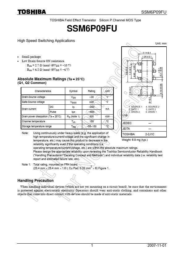
SSM6P09FU Overview
Key Specifications
Max Operating Temp: 150 °C
Key Features
- Small package
- Low Drain-Source ON resistance
Max Operating Temp: 150 °C
| Seller | Inventory | Price Breaks | Buy |
|---|---|---|---|
| Win Source | 9000 | - | View Offer |
| Run Hong Electronics | 7668 | 1+ : 0.0688 USD | View Offer |
| Part Number | Manufacturer | Description |
|---|---|---|
| AP9563GH | Advanced Power Electronics Corp | P-CHANNEL ENHANCEMENT MODE POWER MOSFET |
| A2SHB | HAOHAI | N-Channel MOSFET |
| FCPF360N65S3R0L | onsemi | N-Channel MOSFET |