TC74AC112F
Features
- High speed: fmax = 170 MHz (typ.) at VCC = 5 V
- Low power dissipation: ICC = 4 μA (max) at Ta = 25°C
- High noise immunity: VNIH = VNIL = 28% VCC (min)
- Symmetrical output impedance: |IOH| = IOL = 24 m A (min)
Capability of driving 50 Ω transmission lines.
- Balanced propagation delays: tp LH ∼- tp HL
- Wide operating voltage range: VCC (opr) = 2 to 5.5 V
- Pin and function patible with 74F112
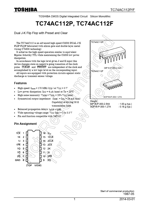
Pin Assignment
TC74AC112P...