TC74AC112P
Features
- High speed: fmax = 170 MHz (typ.) at VCC = 5 V
- Low power dissipation: ICC = 4 μA (max) at Ta = 25°C
- High noise immunity: VNIH = VNIL = 28% VCC (min)
- Symmetrical output impedance: |IOH| = IOL = 24 m A (min)
Capability of driving 50 Ω transmission lines.
- Balanced propagation delays: tp LH ∼- tp HL
- Wide operating voltage range: VCC (opr) = 2 to 5.5 V
- Pin and function patible with 74F112
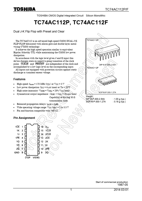
Pin Assignment
TC74AC112P TC74AC112F
Weight DIP16-P-300-2.54A SOP16-P-300-1.27A
: 1.00 g (typ.) : 0.18 g (typ.)
Start of mercial production
1987-05
2014-03-01
IEC Logic Symbol
TC74AC112P/F
Truth Table
Inputs
CLR...