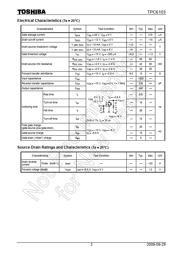
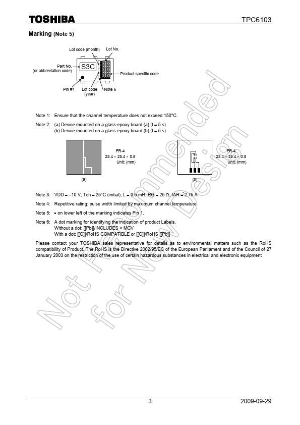
The following content is an automatically extracted verbatim text
from the original manufacturer datasheet and is provided for reference purposes only.
View original datasheet text
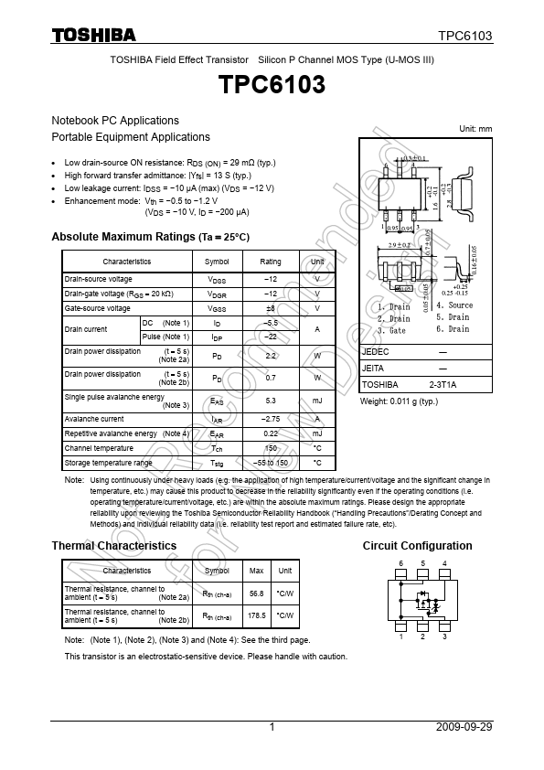
TPC6103
TOSHIBA Field Effect Transistor Silicon P Channel MOS Type (U-MOS III)
TPC6103
Notebook PC Applications Portable Equipment Applications
Unit: mm
• Low drain-source ON resistance: RDS (ON) = 29 mΩ (typ.) • High forward transfer admittance: |Yfs| = 13 S (typ.) • Low leakage current: IDSS = −10 μA (max) (VDS = −12 V) • Enhancement mode: Vth = −0.5 to −1.2 V
(VDS = −10 V, ID = −200 μA)
Absolute Maximum Ratings (Ta = 25°C)
Characteristics
Symbol
Rating
Unit
Drain-source voltage
Drain-gate voltage (RGS = 20 kΩ)
Gate-source voltage
Drain current
DC (Note 1) Pulse (Note 1)
Drain power dissipation
(t = 5 s) (Note 2a)
Drain power dissipation
(t = 5 s) (Note 2b)
Single pulse avalanche energy (Note 3)
VDSS VDGR VGSS
ID IDP PD
PD
EAS
−12
V
−12
V
±8
V
−5.5 A
−22
2.