Click to expand full text
MOSFETs Silicon P-Channel MOS (U-MOS)
SSM6J511NU
1. Applications
• Power Management Switches
2. Features
(1) 1.8 V gate drive voltage. (2) Low drain-source on-resistance
: RDS(ON) = 13.5 mΩ (max) (@VGS = -2.5 V) RDS(ON) = 10 mΩ (max) (@VGS = -4.5 V)
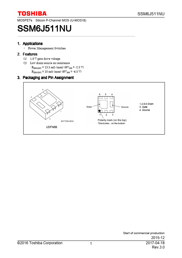
3. Packaging and Pin Assignment
UDFN6B
SSM6J511NU
1.2.5.6 Drain 3. Gate 4. Source
©2016 Toshiba Corporation
1
Start of commercial production
2015-12
2017-04-18 Rev.3.0
SSM6J511NU
4. Absolute Maximum Ratings (Note) (Unless otherwise specified, Ta = 25 )
Characteristics
Symbol
Rating
Unit
Drain-source voltage
VDSS -12 V
Gate-source voltage
VGSS
±10
Drain current (DC)
(Note 1)
ID
-14 A
Drain current (pulsed)
(Note 1), (Note 2)
IDP
-40
Power dissipation
(Note 3)
PD
1.25 W
Power dissipation
(t ≤ 10 s)
(Note 3)
PD
2.